AD5625BRUZ Analog Devices Inc, AD5625BRUZ Datasheet - Page 5
AD5625BRUZ
Manufacturer Part Number
AD5625BRUZ
Description
IC DAC NANO 12BIT QUAD 14-TSSOP
Manufacturer
Analog Devices Inc
Series
nanoDAC™r
Specifications of AD5625BRUZ
Data Interface
I²C, Serial
Settling Time
3µs
Number Of Bits
12
Number Of Converters
4
Voltage Supply Source
Single Supply
Operating Temperature
-40°C ~ 105°C
Mounting Type
Surface Mount
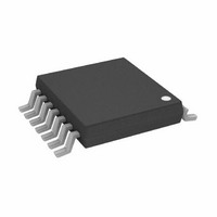
Package / Case
14-TSSOP
Resolution (bits)
12bit
Sampling Rate
333kSPS
Input Channel Type
Serial
Supply Voltage Range - Analogue
2.7V To 5.5V
Supply Current
1.9mA
Digital Ic Case Style
TSSOP
No.
RoHS Compliant
Number Of Channels
4
Resolution
12b
Conversion Rate
333KSPS
Interface Type
Serial (2-Wire/I2C)
Single Supply Voltage (typ)
3.3/5V
Dual Supply Voltage (typ)
Not RequiredV
Architecture
Resistor-String
Power Supply Requirement
Single
Output Type
Voltage
Single Supply Voltage (min)
2.7V
Single Supply Voltage (max)
5.5V
Dual Supply Voltage (min)
Not RequiredV
Dual Supply Voltage (max)
Not RequiredV
Operating Temp Range
-40C to 105C
Operating Temperature Classification
Industrial
Mounting
Surface Mount
Pin Count
14
Lead Free Status / RoHS Status
Lead free / RoHS Compliant
Power Dissipation (max)
-
Lead Free Status / Rohs Status
Compliant


SPECIFICATIONS—AD5665/AD5625
V
Table 3.
Parameter
STATIC PERFORMANCE
OUTPUT CHARACTERISTICS
REFERENCE INPUTS
LOGIC INPUTS (ADDRx, CLR, LDAC, POR)
LOGIC INPUTS (SDA, SCL)
DD
AD5665
AD5625
Zero-Code Error
Offset Error
Full-Scale Error
Gain Error
Zero-Code Error Drift
Gain Temperature Coefficient
DC Power Supply Rejection Ratio
DC Crosstalk (External Reference)
DC Crosstalk (Internal Reference)
Output Voltage Range
Capacitive Load Stability
DC Output Impedance
Short-Circuit Current
Power-Up Time
Reference Current
Reference Input Range
Reference Input Impedance
I
V
V
C
V
I
V
V
C
V
IN
IN
INL
INH
IN
HYST
INL
INH
IN
HYST
= 2.7 V to 5.5 V; R
, Input Current
, Input Current
Resolution
Relative Accuracy
Differential Nonlinearity
Resolution
Relative Accuracy
Differential Nonlinearity
, Pin Capacitance
, Pin Capacitance
, Input Low Voltage
, Input Low Voltage
, Input High Voltage
, Input High Voltage
, Input Hysteresis
, Input Hysteresis
2
L
= 2 kΩ to GND; C
3
3
3
L
= 200 pF to GND; V
Min
16
12
0
0.75
0.85 × V
0.1 × V
0.7 × V
0.1 × V
0.05 × V
DD
DD
DD
DD
DD
B Grade
Typ
±8
±0.5
2
±1
±0.1
±2
−100
0.5
−0.1
±2.5
15
10
8
25
20
10
2
10
30
4
210
26
2
2
Rev. B | Page 5 of 36
AD5625R/AD5645R/AD5665R, AD5625/AD5665
REFIN
10
Max
±16
±1
±1
±0.25
±10
±0.5
±1
V
260
V
±1
0.15 × V
±1
0.3 × V
= V
DD
DD
DD
; all specifications T
DD
DD
Unit
Bits
LSB
LSB
Bits
LSB
LSB
mV
mV
% FSR
% FSR
μV/°C
ppm
dB
μV
μV/mA
μV
μV
μV/mA
μV
V
nF
nF
Ω
mA
μs
μA
V
kΩ
μA
V
V
pF
V
μA
V
V
pF
V
V
Test Conditions/Comments
Guaranteed monotonic by design
Guaranteed monotonic by design
All 0s loaded to DAC register
All 1s loaded to DAC register
Of FSR/°C
DAC code = midscale; V
Due to full-scale output change,
R
Due to load current change
Due to powering down (per channel)
Due to full-scale output change,
R
Due to load current change
Due to powering down (per channel)
R
R
V
Coming out of power-down mode; V
V
High speed mode
Fast mode
L
L
L
L
DD
REF
MIN
= 2 kΩ to GND or V
= 2 kΩ to GND or V
= ∞
= 2 kΩ
= 5 V
= V
to T
DD
MAX
= 5.5 V
, unless otherwise noted.
DD
DD
DD
= 5 V ± 10%
1
DD
= 5 V
Related parts for AD5625BRUZ
Image
Part Number
Description
Manufacturer
Datasheet
Request
R

Part Number:
Description:
±1.7g Dual-Axis IMEMS Accelerometer Evaluation Board
Manufacturer:
Analog Devices Inc
Datasheet:

Part Number:
Description:
Inertial Sensor Evaluation System
Manufacturer:
Analog Devices Inc
Datasheet:
Part Number:
Description:
Manufacturer:
Analog Devices Inc
Datasheet:
Part Number:
Description:
Manufacturer:
Analog Devices Inc
Datasheet:
Part Number:
Description:
Manufacturer:
Analog Devices Inc
Datasheet:
Part Number:
Description:
Manufacturer:
Analog Devices Inc
Datasheet:
Part Number:
Description:
Manufacturer:
Analog Devices Inc
Datasheet:
Part Number:
Description:
Manufacturer:
Analog Devices Inc
Datasheet:
Part Number:
Description:
Manufacturer:
Analog Devices Inc
Datasheet:
Part Number:
Description:
Manufacturer:
Analog Devices Inc
Datasheet:
Part Number:
Description:
Manufacturer:
Analog Devices Inc
Datasheet:
Part Number:
Description:
Manufacturer:
Analog Devices Inc
Datasheet:
Part Number:
Description:
Manufacturer:
Analog Devices Inc
Datasheet: