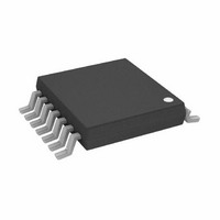
AD5625BRUZ Analog Devices Inc, AD5625BRUZ Datasheet - Page 22

AD5625BRUZ
Manufacturer Part Number
AD5625BRUZ
Description
IC DAC NANO 12BIT QUAD 14-TSSOP
Manufacturer
Analog Devices Inc
Series
nanoDAC™r
Specifications of AD5625BRUZ
Data Interface
I²C, Serial
Settling Time
3µs
Number Of Bits
12
Number Of Converters
4
Voltage Supply Source
Single Supply
Operating Temperature
-40°C ~ 105°C
Mounting Type
Surface Mount
Package / Case
14-TSSOP
Resolution (bits)
12bit
Sampling Rate
333kSPS
Input Channel Type
Serial
Supply Voltage Range - Analogue
2.7V To 5.5V
Supply Current
1.9mA
Digital Ic Case Style
TSSOP
No.
RoHS Compliant
Number Of Channels
4
Resolution
12b
Conversion Rate
333KSPS
Interface Type
Serial (2-Wire/I2C)
Single Supply Voltage (typ)
3.3/5V
Dual Supply Voltage (typ)
Not RequiredV
Architecture
Resistor-String
Power Supply Requirement
Single
Output Type
Voltage
Single Supply Voltage (min)
2.7V
Single Supply Voltage (max)
5.5V
Dual Supply Voltage (min)
Not RequiredV
Dual Supply Voltage (max)
Not RequiredV
Operating Temp Range
-40C to 105C
Operating Temperature Classification
Industrial
Mounting
Surface Mount
Pin Count
14
Lead Free Status / RoHS Status
Lead free / RoHS Compliant
Power Dissipation (max)
-
Lead Free Status / Rohs Status
Compliant
AD5625R/AD5645R/AD5665R, AD5625/AD5665
THEORY OF OPERATION
DIGITAL-TO-ANALOG CONVERTER (DAC)
The AD56x5R/AD56x5 DACs are fabricated on a CMOS
process. The AD56x5 does not have an internal reference, and
the DAC architecture is shown in Figure 54. The AD56x5R does
have an internal reference and can be configured for use with
either an internal or external reference (see Figure 54 and
Figure 55).
Because the input coding to the DAC is straight binary, the ideal
output voltage when using an external reference is given by
The ideal output voltage when using the internal reference is
given by
where:
D is the decimal equivalent of the binary code that is loaded to
the DAC register, as follows:
N is the DAC resolution.
0 to 4095 for AD5625R/AD5625 (12-bit).
0 to 16,383 for AD5645R (14-bit).
0 to 65,535 for AD5665R/AD5665 (16-bit).
V
1
BY V
Figure 55. Internal Configuration When Using the Internal Reference
Figure 54. Internal Configuration When Using an External Reference
CAN BE OVERDRIVEN
REFIN
V
V
OUT
OUT
REFIN
1.25V INTERNAL
/V
REFERENCE
REFOUT
/V
=
=
REFOUT
V
2
REGISTER
REGISTER
×
REFIN
DAC
DAC
V
REFOUT
.
1
V
REFIN
⎛ ×
REF
BUFFER
⎜
⎝
2
D
/V
N
⎛ ×
REFOUT
⎜
⎝
⎞
⎟
⎠
2
D
N
RESISTOR
RESISTOR
STRING
REF (+)
REF (–)
STRING
REF (+)
REF (–)
⎞
⎟
⎠
GND
GND
OUTPUT
AMPLIFIER
GAIN = ×2
OUTPUT
AMPLIFIER
GAIN = ×2
V
V
OUT
OUT
Rev. B | Page 22 of 36
RESISTOR STRING
The resistor string is shown in Figure 56. It is simply a string of
resistors, each of value R. The code loaded to the DAC register
determines at which node on the string the voltage is tapped off
to be fed into the output amplifier. The voltage is tapped off by
closing one of the switches connecting the string to the amplifier.
Because it is a string of resistors, it is guaranteed monotonic.
OUTPUT AMPLIFIER
The output buffer amplifier can generate rail-to-rail voltages on its
output, which gives an output range of 0 V to V
load of 2 kΩ in parallel with 1000 pF to GND. The source and
sink capabilities of the output amplifier are shown in Figure 38
and Figure 39. The slew rate is 1.8 V/μs with a ¼ to ¾ full-scale
settling time of 7 μs.
INTERNAL REFERENCE
The AD5625R/AD5645R/AD5665R feature an on-chip reference.
Versions without the R suffix require an external reference. The
on-chip reference is off at power-up and is enabled via a write to a
control register. See the Internal Reference Setup section for details.
Versions packaged in a 10-lead LFCSP have a 1.25 V reference
or a 2.5 V reference, giving a full-scale output of 2.5 V or 5 V,
depending on the model selected (see the Ordering Guide). These
parts can be operated with a V
packaged in a 14-lead TSSOP have a 2.5 V reference, giving a
full-scale output of 5 V. Parts are functional with a V
of 2.7 V to 5.5 V, but, with a V
output is clamped to V
of models. The internal reference associated with each part is
available at the V
A buffer is required if the reference output is used to drive
external loads. When using the internal reference, it is recom-
mended that a 100 nF capacitor be placed between the reference
output and GND for reference stability.
R
R
R
R
R
REFOUT
Figure 56. Resistor String
DD
pin (available on R suffix versions only).
. See the Ordering Guide for a full list
DD
DD
supply of 2.7 V to 5.5 V. Versions
supply of less than 5 V, the
TO OUTPUT
AMPLIFIER
DD
. It can drive a
DD
supply


