AD876JR Analog Devices Inc, AD876JR Datasheet
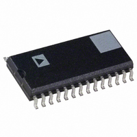
IC ADC 10BIT 20MSPS CMOS 28-SOIC

AD876JR

Manufacturer Part Number
AD876JR
Description
IC ADC 10BIT 20MSPS CMOS 28-SOIC
Manufacturer
Analog Devices Inc
Datasheet

Specifications of AD876JR

Data Interface
Parallel
Rohs Status
RoHS non-compliant
Number Of Bits
10
Sampling Rate (per Second)
20M
Number Of Converters
7
Power Dissipation (max)
190mW
Voltage Supply Source
Analog and Digital, Dual ±
Operating Temperature
0°C ~ 70°C
Mounting Type
Surface Mount
Package / Case
28-SOIC (0.300", 7.50mm Width)
Resolution (bits)
10bit
Sampling Rate
20MSPS
Input Channel Type
Single Ended
Supply Current
20mA
Digital Ic Case Style
SOIC
No. Of Pins
28
Lead Free Status / RoHS Status
Contains lead / RoHS non-compliant

Available stocks

Company
Part Number
Manufacturer
Quantity
Price
Part Number:
AD876JR
Manufacturer:
QUCKLOGIC
Quantity:
6
Part Number:
AD876JR
Manufacturer:
AD
Quantity:
4 350
Part Number:
AD876JR
Manufacturer:
ADI/亚德诺
Quantity:
20 000
a
PRODUCT DESCRIPTION
The AD876 is a CMOS, 160 mW, 10-bit, 20 MSPS analog-to-
digital converter (ADC). The AD876 has an on-chip input
sample-and-hold amplifier. By implementing a multistage pipe-
lined architecture with output error correction logic, the AD876
offers accurate performance and guarantees no missing codes
over the full operating temperature range. Force and sense con-
nections to the reference inputs minimize external voltage drops.
The AD876 can be placed into a standby mode of operation
reducing the power below 50 mW. The AD876’s digital I/O
interfaces to either +5 V or +3.3 V logic. Digital output pins
can be placed in a high impedance state; the format of the out-
put is straight binary coding.
The AD876’s speed, resolution and single-supply operation
ideally suit a variety of applications in video, multimedia, imag-
ing, high speed data acquisition and communications. The
AD876’s low power and single-supply operation satisfy require-
ments for high speed portable applications. Its speed and reso-
lution ideally suit charge coupled device (CCD) input systems
such as color scanners, digital copiers, electronic still cameras
and camcorders.
REV. B
Information furnished by Analog Devices is believed to be accurate and
reliable. However, no responsibility is assumed by Analog Devices for its
use, nor for any infringements of patents or other rights of third parties
which may result from its use. No license is granted by implication or
otherwise under any patent or patent rights of Analog Devices.
FEATURES
CMOS 10-Bit 20 MSPS Sampling A/D Converter
Pin-Compatible 8-Bit Option
Power Dissipation: 160 mW
+5 V Single Supply Operation
Differential Nonlinearity: 0.5 LSB
Guaranteed No Missing Codes
Power Down (Standby) Mode
Three-State Outputs
Digital I/Os Compatible with +5 V or +3.3 V Logic
Adjustable Reference Input
Small Size: 28-Lead SOIC, 28-Lead SSOP, or 48-Lead
Thin Quad Flatpack (TQFP)
The AD876 comes in a space saving 28-lead SOIC and 48-lead
thin quad flatpack (TQFP) and is specified over the commercial
(0 C to +70 C) temperature range.
PRODUCT HIGHLIGHTS
Low Power
The AD876 at 160 mW consumes a fraction of the power of
presently available 8- or 10-bit, video speed converters. Power-
down mode and single-supply operation further enhance its
desirability in low power, battery operated applications such
as electronic still cameras, camcorders and communication
systems.
Very Small Package
The AD876 comes in a 28-lead SOIC, 28-lead SSOP, and 48-
lead surface mount, thin quad flat package. The TQFP package
is ideal for very tight, low headroom designs.
Digital I/O Functionality
The AD876 offers three-state output control.
Pin Compatible Upgrade Path
The AD876 offers the option of laying out designs for eight
bits and migrating to 10-bit resolution if prototype results
warrant.
One Technology Way, P.O. Box 9106, Norwood, MA 02062-9106, U.S.A.
Tel: 781/329-4700
Fax: 781/326-8703
REFBS
REFTF
REFTS
REFBF
AIN
SHA
CML
CLK
AD876
A/D
FUNCTIONAL BLOCK DIAGRAM
SHA
10-Bit 20 MSPS 160 mW
D/A
World Wide Web Site: http://www.analog.com
GAIN
AV
AV
CMOS A/D Converter
DD
SS
OUTPUT BUFFERS
A/D
DV
SHA
CORRECTION LOGIC
DV
SS
DD
D/A
DRV
DRV
GAIN
DD
SS
© Analog Devices, Inc., 1998
A/D
SHA
D/A
AD876
GAIN
A/D
THREE-
(MSB)
D9
D0
(LSB)
STBY
STATE

Related parts for AD876JR

AD876JR Summary of contents

Page 1

FEATURES CMOS 10-Bit 20 MSPS Sampling A/D Converter Pin-Compatible 8-Bit Option Power Dissipation: 160 Single Supply Operation Differential Nonlinearity: 0.5 LSB Guaranteed No Missing Codes Power Down (Standby) Mode Three-State Outputs Digital I/Os Compatible with +5 ...

Page 2

... MHz Input Frequency. Specifications subject to change without notice. See Definition of Specifications for additional information with +5.0 V, DRV MIN MAX MSPS, unless otherwise noted) CLOCK AD876JR-8 Min Typ Max Min 8 0.3 1.0 0.1 0.75 GUARANTEED 0.1 0.1 2 5.0 3.5 4 ...

Page 3

DIGITAL SPECIFICATIONS Parameter LOGIC INPUT High Level Input Voltage Low Level Input Voltage High Level Input Current Low Level Input Current Low Level Input Current (CLK Only) Input Capacitance LOGIC OUTPUTS High Level Output Voltage ( ...

Page 4

... TOP VIEW D5 8 (Not to Scale DRV PINS D0 AND D1 ARE LEFT OPEN FOR THE AD876JR CONNECT PIN FUNCTION DESCRIPTIONS TQFP Pin No. Type Name and Function 1 DO Least Significant Bit. 2–5 DO Data Bits 1 through 4. 8–11 Data Bits 5 through Most Significant Bit THREE-STATE = LOW ...

Page 5

... Volts Model –0.5 +6.5 Volts AD876JR –0.5 +0.5 Volts AD876JST-Reel +70 C –0.5 +6.5 Volts AD876JR-8 –0.5 +6.5 Volts AD876AR –0.5 +6.5 Volts AD876ARS +150 C AD876JRS –65 +150 C AD876JRS-8 +300 DRV DRV SS b) Three-State, Standby AV DD REFTF AV DD REFTS AV DD ...

Page 6

Performance Characteristics AD876 1 0.5 0 –0.5 – 128 192 256 320 384 448 512 576 CODE OFFSET Figure 3. AD876 Typical DNL 2 0 –2 –4 –6 –8 – FREQUENCY – MHz Figure 4. ...

Page 7

... THD = –64.12 SNR = 48.73 SINAD = 48.61 SFDR = –68. Figure 9. AD876JR-8 Typical FFT (f AIN = –0.5 dB MSPS) CLOCK HARMONICS (dBc) 2ND –68.91 6TH –80.55 3RD –73.92 7TH –82.02 4TH –68.67 8TH –81.02 5TH –73.26 9TH – ...

Page 8

AD876 analog ground can lower the ac source impedance. The value of this capacitance will depend on the source resistance and the required signal bandwidth. The input span of the AD876 is a function of the reference voltages. For more ...

Page 9

Figure 16 shows the equivalent input structure for the AD876 reference pins. There is approximately 5 both the REFTF and REFBT pins and the reference ladder. If the force-sense connections are not used, the voltage drop across the 5 resistors ...

Page 10

AD876 C3 0 REFT 1/2 C2 AD826 0 0 REFB 4 1/2 0.1 F AD826 Figure 19. Kelvin Connected Reference Using the AD826 By ...

Page 11

Table I. Output Data Format Approx. THREE- DATA AIN (V) STATE > ...

Page 12

AD876 STBY +5VD VP6 +5VD C50 JP4 JP1 JP2 VP8 C62 0.1 F REFTS VP3 REFTS REFTF REFBF REFBS VP4 REFBS REFTF REFBF VP1 VP2 R16 R17 1k 1.13k DC_IN R18 R14 1k ...

Page 13

Figure 24. Silkscreen Layer, Component Side PCXB Layout Figure 25. Silkscreen Layer, Circuit Side PCB Layout REV. B –13– AD876 ...

Page 14

AD876 Figure 26. Component Side PCB Layout Figure 27. Circuit Side PCB Layout –14– REV. B ...

Page 15

REV. B Figure 28. Ground Layer PCB Layout Figure 29. Power Layer PCB Layout –15– AD876 ...

Page 16

AD876 0.0118 (0.30) 0.0040 (0.10) 0.02 (0.5 SEATING 0.004 (0.1 (3.5 0.005 +0.002 –0.0008 (0.127 +0.05 –0.02) 0.078 (1.98) 0.068 (1.73) 0.008 (0.203) 0.002 (0.050) OUTLINE DIMENSIONS Dimensions shown in inches and (mm). R-28 28-Lead Wide Body (SOIC) 0.7125 (18.10) ...

Related keywords