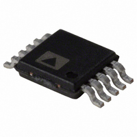
AD7790BRMZ Analog Devices Inc, AD7790BRMZ Datasheet - Page 14

AD7790BRMZ
Manufacturer Part Number
AD7790BRMZ
Description
IC ADC 16BIT SIGMA-DELTA 10-MSOP
Manufacturer
Analog Devices Inc
Datasheet
1.AD7790BRMZ-REEL.pdf
(20 pages)
Specifications of AD7790BRMZ
Data Interface
DSP, MICROWIRE™, QSPI™, Serial, SPI™
Number Of Bits
16
Sampling Rate (per Second)
120
Number Of Converters
1
Power Dissipation (max)
230µW
Voltage Supply Source
Single Supply
Operating Temperature
-40°C ~ 105°C
Mounting Type
Surface Mount
Package / Case
10-TFSOP (0.118", 3.00mm Width)
Resolution (bits)
16bit
Input Channel Type
Differential
Supply Current
145µA
Digital Ic Case Style
SOP
No. Of Pins
10
Operating Temperature Range
-40°C To +105°C
Number Of Elements
1
Resolution
16Bit
Architecture
Delta-Sigma
Sample Rate
0.12KSPS
Input Polarity
Bipolar
Input Type
Voltage
Rated Input Volt
±2.5V
Differential Input
Yes
Power Supply Requirement
Single
Single Supply Voltage (typ)
3.3/5V
Single Supply Voltage (min)
2.5V
Single Supply Voltage (max)
5.25V
Dual Supply Voltage (typ)
Not RequiredV
Dual Supply Voltage (min)
Not RequiredV
Dual Supply Voltage (max)
Not RequiredV
Power Dissipation
225uW
Integral Nonlinearity Error
±15ppm of FSR
Operating Temp Range
-40C to 105C
Operating Temperature Classification
Industrial
Mounting
Surface Mount
Pin Count
10
Package Type
MSOP
Input Signal Type
Differential
Lead Free Status / RoHS Status
Lead free / RoHS Compliant
Lead Free Status / RoHS Status
Lead free / RoHS Compliant, Lead free / RoHS Compliant
Available stocks
Company
Part Number
Manufacturer
Quantity
Price
Company:
Part Number:
AD7790BRMZ
Manufacturer:
ADI
Quantity:
1 000
Part Number:
AD7790BRMZ
Manufacturer:
ADI/亚德诺
Quantity:
20 000
Company:
Part Number:
AD7790BRMZ-REEL
Manufacturer:
AMD
Quantity:
101
Company:
Part Number:
AD7790BRMZ-REEL
Manufacturer:
ADI
Quantity:
1 000
AD7790
DIGITAL INTERFACE
As previously outlined, the AD7790’s programmable functions
are controlled using a set of on-chip registers. Data is written to
these registers via the part’s serial interface and read access to
the on-chip registers is also provided by this interface. All com-
munications with the part must start with a write to the
communications register. After power-on or reset, the device
expects a write to its communications register. The data written
to this register determines whether the next operation is a read
operation or a write operation and also determines to which
register this read or write operation occurs. Therefore, write
access to any of the other registers on the part begins with a
write operation to the communications register followed by a
write to the selected register. A read operation from any other
register (except when continuous read mode is selected) starts
with a write to the communications register followed by a read
operation from the selected register.
The AD7790’s serial interface consists of four signals: CS , DIN,
SCLK, and DOUT/ RDY . The DIN line is used to transfer data
into the on-chip registers while DOUT/ RDY is used for access-
ing from the on-chip registers. SCLK is the serial clock input for
the device and all data transfers (either on DIN or DOUT/ RDY )
occur with respect to the SCLK signal. The DOUT/ RDY pin
operates as a Data Ready signal also, the line going low when a
new data-word is available in the output register. It is reset high
when a read operation from the data register is complete. It also
goes high prior to the updating of the data register to indicate
when not to read from the device to ensure that a data read is
not attempted while the register is being updated. CS is used to
select a device. It can be used to decode the AD7790 in systems
where several components are connected to the serial bus.
Figure 3 and Figure 4 show timing diagrams for interfacing to
the AD7790 with CS being used to decode the part. Figure 3
shows the timing for a read operation from the AD7790’s output
Rev. 0 | Page 14 of 20
shift register while Figure 4 shows the timing for a write opera-
tion to the input shift register. In all modes except continuous
read mode, it is possible to read the same word from the data
register several times even though the DOUT/ RDY line returns
high after the first read operation. However, care must be taken
to ensure that the read operations have been completed before
the next output update occurs. In continuous read mode, the
data register can be read only once.
The serial interface can operate in 3-wire mode by tying CS low.
In this case, the SCLK, DIN, and DOUT/ RDY lines are used to
communicate with the AD7790. The end of the conversion can
be monitored using the RDY bit in the status register. This
scheme is suitable for interfacing to microcontrollers. If CS is
required as a decoding signal, it can be generated from a port
pin. For microcontroller interfaces, it is recommended that
SCLK idles high between data transfers.
The AD7790 can be operated with CS being used as a frame
synchronization signal. This scheme is useful for DSP interfaces.
In this case, the first bit (MSB) is effectively clocked out by CS
since CS would normally occur after the falling edge of SCLK in
DSPs. The SCLK can continue to run between data transfers,
provided the timing numbers are obeyed.
The serial interface can be reset by writing a series of 1s on the
DIN input. If a Logic 1 is written to the AD7790 line for at least
32 serial clock cycles, the serial interface is reset. This ensures
that in 3-wire systems, the interface can be reset to a known
state if the interface gets lost due to a software error or some
glitch in the system. Reset returns the interface to the state in
which it is expecting a write to the communications register.
This operation resets the contents of all registers to their power-
on values.
The AD7790 can be configured to continuously convert or to
perform a single conversion. See Figure 8 through Figure 10.


