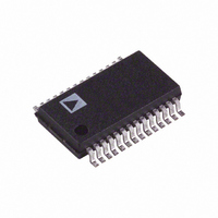
AD9200JRSZ Analog Devices Inc, AD9200JRSZ Datasheet - Page 4

AD9200JRSZ
Manufacturer Part Number
AD9200JRSZ
Description
IC ADC 10BIT CMOS 20MSPS 28-SSOP
Manufacturer
Analog Devices Inc
Datasheet
1.AD9200ARSZRL.pdf
(24 pages)
Specifications of AD9200JRSZ
Data Interface
Parallel
Number Of Bits
10
Sampling Rate (per Second)
20M
Number Of Converters
9
Power Dissipation (max)
100mW
Voltage Supply Source
Single Supply
Operating Temperature
0°C ~ 70°C
Mounting Type
Surface Mount
Package / Case
28-SSOP (0.200", 5.30mm Width)
Resolution (bits)
10bit
Sampling Rate
20MSPS
Input Channel Type
Differential, Single Ended
Supply Voltage Range - Analog
2.7V To 5.5V
Number Of Elements
1
Resolution
10Bit
Architecture
Pipelined
Sample Rate
20MSPS
Input Polarity
Unipolar
Input Type
Voltage
Rated Input Volt
±0.5/±1V
Differential Input
Yes
Power Supply Requirement
Analog and Digital
Single Supply Voltage (typ)
3V
Single Supply Voltage (min)
2.7V
Single Supply Voltage (max)
5.5V
Dual Supply Voltage (typ)
Not RequiredV
Dual Supply Voltage (min)
Not RequiredV
Dual Supply Voltage (max)
Not RequiredV
Power Dissipation
100mW
Differential Linearity Error
±1LSB
Integral Nonlinearity Error
±2LSB
Operating Temp Range
0C to 70C
Operating Temperature Classification
Commercial
Mounting
Surface Mount
Pin Count
28
Package Type
SSOP
Lead Free Status / RoHS Status
Lead free / RoHS Compliant
Lead Free Status / RoHS Status
Lead free / RoHS Compliant, Lead free / RoHS Compliant
Available stocks
Company
Part Number
Manufacturer
Quantity
Price
Part Number:
AD9200JRSZ
Manufacturer:
ADI/亚德诺
Quantity:
20 000
AD9200
CAUTION
ESD (electrostatic discharge) sensitive device. Electrostatic charges as high as 4000 V readily
accumulate on the human body and test equipment and can discharge without detection.
Although the AD9200 features proprietary ESD protection circuitry, permanent damage may
occur on devices subjected to high energy electrostatic discharges. Therefore, proper ESD
precautions are recommended to avoid performance degradation or loss of functionality.
ABSOLUTE MAXIMUM RATINGS*
Parameter
AVDD
DRVDD
AVSS
AVDD
MODE
CLK
Digital Outputs
AIN
VREF
REFSENSE
REFTF, REFTB
REFTS, REFBS
Junction Temperature
Storage Temperature
Lead Temperature
10 sec
a. D0–D9, OTR
f. CLAMPIN
With
Respect
to
AVSS
DRVSS
DRVSS
DRVDD –6.5
AVSS
AVSS
DRVSS
AVSS
AVSS
AVSS
AVSS
AVSS
AVDD
AVSS
AVDD
AVSS
d. AIN
AVDD
AVSS
–0.3
–0.3
Min
–0.3
–0.3
–0.3
–0.3
–0.3
–0.3
–0.3
–0.3
–0.3
–65
DRVDD
DRVSS
DRVSS
Max
+6.5
+6.5
+0.3
+6.5
AVDD + 0.3
AVDD + 0.3
DRVDD + 0.3 V
AVDD + 0.3
AVDD + 0.3
AVDD + 0.3
AVDD + 0.3
AVDD + 0.3
+150
+150
+300
b. Three-State, Standby, Clamp
g. MODE
Figure 2. Equivalent Circuits
AVDD
AVSS
REFBS
REFBF
Units
V
V
V
V
V
V
V
V
V
V
V
AVSS
AVDD
C
C
C
AVDD
AVDD
–4–
*Stresses above those listed under Absolute Maximum Ratings may cause perma-
Model
AD9200JRS
AD9200ARS
AD9200JST
AD9200KST
AD9200JRSRL
AD9200ARSRL –40 C to +85 C 28-Lead SSOP (Reel) RS-28
AD9200JSTRL
AD9200KSTRL 0 C to +70 C
AD9200 SSOP-EVAL
AD9200 LQFP-EVAL
*RS = Shrink Small Outline; ST = Thin Quad Flatpack.
AVSS
nent damage to the device. This is a stress rating only; functional operation of the
device at these or any other conditions above those indicated in the operational
sections of this specification is not implied. Exposure to absolute maximum
ratings for extended periods may effect device reliability.
AVSS
AVSS
AVDD
h. REFSENSE
AVDD
AVSS
e. Reference
Temperature
Range
0 C to +70 C
–40 C to +85 C 28-Lead SSOP
0 C to +70 C
0 C to +70 C
0 C to +70 C
0 C to +70 C
ORDERING GUIDE
REFTS
REFTF
AVSS
AVDD
AVDD
AVDD
Package
Description
28-Lead SSOP
48-Lead LQFP
48-Lead LQFP
28-Lead SSOP (Reel) RS-28
48-Lead LQFP (Reel) ST-48
48-Lead LQFP (Reel) ST-48
Evaluation Board
Evaluation Board
c. CLK
WARNING!
i. VREF
AVSS
AVSS
AVDD
AVSS
AVSS
AVDD
ESD SENSITIVE DEVICE
Package
Options*
RS-28
RS-28
ST-48
ST-48
REV. E


