ADC12048CIV/NOPB National Semiconductor, ADC12048CIV/NOPB Datasheet - Page 9
ADC12048CIV/NOPB
Manufacturer Part Number
ADC12048CIV/NOPB
Description
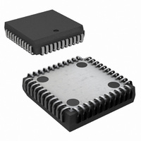
IC ADC 12BIT+SIGN 8-CH 44-PLCC
Manufacturer
National Semiconductor
Datasheet
1.ADC12048CIVNOPB.pdf
(32 pages)
Specifications of ADC12048CIV/NOPB
Number Of Bits
12
Sampling Rate (per Second)
216k
Data Interface
Parallel
Number Of Converters
1
Power Dissipation (max)
875mW
Voltage Supply Source
Analog and Digital
Operating Temperature
-40°C ~ 85°C
Mounting Type
Surface Mount
Package / Case
44-LCC (J-Lead)
Leaded Process Compatible
Yes
Rohs Compliant
Yes
Peak Reflow Compatible (260 C)
Yes
Lead Free Status / RoHS Status
Lead free / RoHS Compliant
Other names
*ADC12048CIV
*ADC12048CIV/NOPB
ADC12048CIV
*ADC12048CIV/NOPB
ADC12048CIV
Available stocks
Company
Part Number
Manufacturer
Quantity
Price
Company:

Part Number:
ADC12048CIV/NOPB
Manufacturer:
Texas Instruments
Quantity:
10 000


Notes on Specifications
Note 7: V
conversion/comparison accuracy. Refer to the Power Supply Considerations section for a detailed discussion.
Note 8: Accuracy is guaranteed when operating at f
Note 9: With the test condition for V
Note 10: Typicals are at T
Note 11: Limits are guaranteed to National’s AOQL (Average Outgoing Quality Level).
Note 12: Positive integral linearity error is defined as the deviation of the analog value, expressed in LSBs, from the straight line that passes through positive
full-scale and zero. For negative integral linearity error, the straight line passes through negative full-scale and zero.
Note 13: Zero error is a measure of the deviation from the mid-scale voltage (a code of zero), expressed in LSB. It is the average value of the code transitions
between −1 to 0 and 0 to +1 (see Figure 8).
Note 14: The DC common-mode error is measured with both inputs shorted together and driven from 0V to 5V. The measured value is referred to the resulting
output value when the inputs are driven with a 2.5V input.
Note 15: Power Supply Sensitivity is measured after an Auto-Zero and Auto Calibration cycle has been completed with V
Note 16: V
Note 17: The ADC12048’s self-calibration technique ensures linearity and offset errors as specified, but noise inherent in the self-calibration process will result in
a repeatability uncertainly of
Note 18: Total Unadjusted Error (TUE) includes offset, full scale linearity and MUX errors.
Note 19: The ADC12048 parts used to gather the information for these curves were auto-calibrated prior to taking the measurements at each test condition. The
auto-calibration cycle cancels any first order drifts due to test conditions. However, each measurement has a repeatability uncertainty error of 0.2 LSB. See (Note
17).
Note 20: The reference input current is a DC average current drawn by the reference input with a full-scale sinewave input. The ADC12048 is continuously
converting with a throughput rate of 206 kHz.
Note 21: These typical curves were measured during continuous conversions with a positive half-scale DC input. A 240 ns RD pulse was applied 25 ns after the
RDY signal went low. The data bus lines were loaded with 2 HC family CMOS inputs (C
Note 22: Any other values placed in the command field are meaningless. However, if a code of 101 or 110 is placed in the command field and the CS, RD and WR
go low at the same time, the ADC12048 will enter a test mode. These test modes are only to be used by the manufacturer of this device. A hardware power-off and
power-on reset must be done to get out of these test modes.
A
+ and V
REFCM
(Reference Voltage Common Mode Range) is defined as
D
+ must be connected together to the same power supply voltage and bypassed with separate capacitors at each V
A
= 25˚C and represent most likely parametric norm.
±
0.20 LSB.
REF
(V
REF
+ − V
CLK
REF
(Continued)
−) given as +4.096V, the 12-bit LSB is 1.000 mV.
= 12 MHz.
9
L
∼ 20 pF).
01238704
A
+ and V
D
+ at the specified extremes.
+
www.national.com
pin to assure
Related parts for ADC12048CIV/NOPB
Image
Part Number
Description
Manufacturer
Datasheet
Request
R

Part Number:
Description:
National Semiconductor [8-Bit D/A Converter]
Manufacturer:
National Semiconductor
Datasheet:
Part Number:
Description:
National Semiconductor [Media Coprocessor]
Manufacturer:
National Semiconductor
Datasheet:
Part Number:
Description:
Digitally Controlled Tone and Volume Circuit with Stereo Audio Power Amplifier, Microphone Preamp Stage and National 3D Sound
Manufacturer:
National Semiconductor
Datasheet:
Part Number:
Description:
Digitally Controlled Tone and Volume Circuit with Stereo Audio Power Amplifier, Microphone Preamp Stage and National 3D Sound
Manufacturer:
National Semiconductor
Datasheet:
Part Number:
Description:
AC97 Rev 2 Codec with Sample Rate Conversion and National 3D Sound
Manufacturer:
National Semiconductor
Part Number:
Description:
Manufacturer:
National Semiconductor
Datasheet:
Part Number:
Description:
Manufacturer:
National Semiconductor
Datasheet:
Part Number:
Description:
General Purpose, Low Voltage, Low Power, Rail-to-Rail Output Operational Amplifiers
Manufacturer:
National Semiconductor
Datasheet:
Part Number:
Description:
8-bit 20 MSPS flash A/D converter.
Manufacturer:
National Semiconductor
Datasheet:
Part Number:
Description:
Low Noise Quad Operational Amplifier
Manufacturer:
National Semiconductor
Datasheet:
Part Number:
Description:
Quad Differential Line Receivers
Manufacturer:
National Semiconductor
Datasheet:
Part Number:
Description:
Quad High Speed Trapezoidal? Bus Transceiver
Manufacturer:
National Semiconductor
Datasheet:
Part Number:
Description:
Dual Line Receiver
Manufacturer:
National Semiconductor
Datasheet:
Part Number:
Description:
TTL to 10k ECL Level Translator with Latch
Manufacturer:
National Semiconductor
Datasheet: