ADC12048CIV/NOPB National Semiconductor, ADC12048CIV/NOPB Datasheet - Page 7
ADC12048CIV/NOPB
Manufacturer Part Number
ADC12048CIV/NOPB
Description
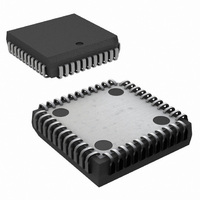
IC ADC 12BIT+SIGN 8-CH 44-PLCC
Manufacturer
National Semiconductor
Datasheet
1.ADC12048CIVNOPB.pdf
(32 pages)
Specifications of ADC12048CIV/NOPB
Number Of Bits
12
Sampling Rate (per Second)
216k
Data Interface
Parallel
Number Of Converters
1
Power Dissipation (max)
875mW
Voltage Supply Source
Analog and Digital
Operating Temperature
-40°C ~ 85°C
Mounting Type
Surface Mount
Package / Case
44-LCC (J-Lead)
Leaded Process Compatible
Yes
Rohs Compliant
Yes
Peak Reflow Compatible (260 C)
Yes
Lead Free Status / RoHS Status
Lead free / RoHS Compliant
Other names
*ADC12048CIV
*ADC12048CIV/NOPB
ADC12048CIV
*ADC12048CIV/NOPB
ADC12048CIV
Available stocks
Company
Part Number
Manufacturer
Quantity
Price
Company:

Part Number:
ADC12048CIV/NOPB
Manufacturer:
Texas Instruments
Quantity:
10 000


t
C
V
V
I
I
V
V
I
C
TPR
IH
IL
OFF
t
t
t
t
Symbol
Symbol
Reference Inputs
IH
IL
OH
OL
IN
Z
CAL
CONV
AcqSYNCOUT
The following specifications apply to the ADC12048 for V
sion mode, f
common-mode voltage, and minimum acquisition time, unless otherwise specified. Boldface limits apply for T
to T
REF
Digital Logic Input/Output Characteristics
The following specifications apply to the ADC12048 for V
sion mode, f
common-mode voltage, and minimum acquisition time, unless otherwise specified. Boldface limits apply for T
to T
Converter AC Characteristics
Digital Timing Characteristics
The following specifications apply to the ADC12048, 13-bit data bus width, V
= 50 pF on data I/O lines
The following specifications apply to the ADC12048 for V
sion mode, f
common-mode voltage, and minimum acquisition time, unless otherwise specified. Boldface limits apply for T
to T
Symbol
Symbol
MAX
MAX
MAX
; all other limits T
; all other limits T
; all other limits T
Reference Input
Capacitance
Logic High Input Voltage
Logic Low Input Voltage
Logic High Input Current
Logic Low Input Current
Logic High Output Voltage
Logic Low Output Voltage
TRI-STATE
Leakage Current
D12–D0 Input Capacitance
CLK
CLK
CLK
Throughput Rate
= 12.0 MHz, R
= 12.0 MHz, R
= 12.0 MHz, R
Auto Zero Time
Full Calibration Time
CLK Duty Cycle
Conversion Time
Acquisition Time
(Programmable)
Parameter
Parameter
®
Output
Parameter
A
A
A
= T
= T
= T
Parameter
(Continued)
J
J
S
S
J
S
= 25˚C
= 25˚C
= 25Ω, source impedance for V
= 25Ω, source impedance for V
= 25˚C
= 25Ω, source impedance for V
V
V
V
V
V
I
V
I
V
V
OUT
OUT
A
A
IN
IN
A
A
OUT
OUT
+ = V
+ = V
+ = V
+ = V
= 5V
= 0V
= −1.6 mA
= 1.6 mA
= 0V
= 5V
Sync-Out Mode
Minimum for 13 Bits
Maximum for 13 Bits
D
D
D
D
+ = 5.5V
+ = 4.5V
+ = 4.5V
+ = 4.5V
Conditions
Conditions
Conditions
A
A
S
+ = V
+ = V
Sync-Out Mode (SYNC Bit =
“0”) 9 Clock Cycles of
Acquisition Time
+ = V
7
D
D
D
REF
REF
+ = 5V, V
+ = 5V, V
REF
+ = 5V, V
Conditions
+ and V
+ and V
+ and V
(Note 10)
REF
REF
Typical
REF
REF
REF
A
REF
4946
+ = V
78
50
44
79
+ = 4.096V, V
+ = 4.096V, V
9
+ = 4.096V, V
− ≤ 1Ω, fully differential input with fixed 2.048V
− ≤ 1Ω, fully differential input with fixed 2.048V
− ≤ 1Ω, fully differential input with fixed 2.048V
(Note 10)
(Note 10)
Typical
Typical
−0.035
0.035
D
10
85
+ = 5V, f
4946 clks + 120 ns
(Note 10)
Typical
78 clks + 120 ns
79 clks + 120 ns
9 clks + 120 ns
REF
REF
REF
222
CLK
(Note 11)
− = 0.0V, 12-bit + sign conver-
− = 0.0V, 12-bit + sign conver-
− = 0.0V, 12-bit + sign conver-
Limits
= 12 MHz, t
40
60
44
(Note 11)
(Note 11)
Limits
Limits
−2.0
±
2.0
0.8
2.0
2.4
0.4
2.0
(Note 11)
Limits
f
A
A
= 3 ns and C
A
= T
= T
= T
www.national.com
clks (max)
clks (max)
clks (max)
clks (max)
clks (max)
µA (max)
µA (max)
µA (max)
J
J
% (max)
V (max)
V (max)
% (min)
V (min)
V (min)
J
(Limit)
(Limit)
(Limit)
= T
= T
(Limit)
Unit
Unit
Unit
= T
Units
pF
pF
%
kHz
MIN
MIN
MIN
L
Related parts for ADC12048CIV/NOPB
Image
Part Number
Description
Manufacturer
Datasheet
Request
R

Part Number:
Description:
National Semiconductor [8-Bit D/A Converter]
Manufacturer:
National Semiconductor
Datasheet:
Part Number:
Description:
National Semiconductor [Media Coprocessor]
Manufacturer:
National Semiconductor
Datasheet:
Part Number:
Description:
Digitally Controlled Tone and Volume Circuit with Stereo Audio Power Amplifier, Microphone Preamp Stage and National 3D Sound
Manufacturer:
National Semiconductor
Datasheet:
Part Number:
Description:
Digitally Controlled Tone and Volume Circuit with Stereo Audio Power Amplifier, Microphone Preamp Stage and National 3D Sound
Manufacturer:
National Semiconductor
Datasheet:
Part Number:
Description:
AC97 Rev 2 Codec with Sample Rate Conversion and National 3D Sound
Manufacturer:
National Semiconductor
Part Number:
Description:
Manufacturer:
National Semiconductor
Datasheet:
Part Number:
Description:
Manufacturer:
National Semiconductor
Datasheet:
Part Number:
Description:
General Purpose, Low Voltage, Low Power, Rail-to-Rail Output Operational Amplifiers
Manufacturer:
National Semiconductor
Datasheet:
Part Number:
Description:
8-bit 20 MSPS flash A/D converter.
Manufacturer:
National Semiconductor
Datasheet:
Part Number:
Description:
Low Noise Quad Operational Amplifier
Manufacturer:
National Semiconductor
Datasheet:
Part Number:
Description:
Quad Differential Line Receivers
Manufacturer:
National Semiconductor
Datasheet:
Part Number:
Description:
Quad High Speed Trapezoidal? Bus Transceiver
Manufacturer:
National Semiconductor
Datasheet:
Part Number:
Description:
Dual Line Receiver
Manufacturer:
National Semiconductor
Datasheet:
Part Number:
Description:
TTL to 10k ECL Level Translator with Latch
Manufacturer:
National Semiconductor
Datasheet: