LMX2371TMX National Semiconductor, LMX2371TMX Datasheet - Page 16
LMX2371TMX
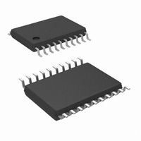
Manufacturer Part Number
LMX2371TMX
Description
IC FREQ SYNTH DUAL 20-TSSOP
Manufacturer
National Semiconductor
Series
PLLatinum™r
Type
PLL Frequency Synthesizerr
Datasheet
1.LMX2372TMX.pdf
(24 pages)
Specifications of LMX2371TMX
Pll
Yes with Bypass
Input
CMOS, TTL
Output
CMOS
Number Of Circuits
1
Ratio - Input:output
3:1
Differential - Input:output
Yes/No
Frequency - Max
2GHz, 1.2GHz
Divider/multiplier
Yes/No
Voltage - Supply
2.7 V ~ 5.5 V
Operating Temperature
-40°C ~ 85°C
Mounting Type
Surface Mount
Package / Case
20-TSSOP
Frequency-max
2GHz
Lead Free Status / RoHS Status
Lead free / RoHS Compliant
Other names
*LMX2371TMX


www.national.com
2.0 Programming Description
2.3.5 PLL Prescaler Select (P_Aux, P_Main)
The LMX2370, LMX2371 and LMX2372 contain two dual modulus prescalers. A 32/33 or a 16/17 prescaler can be selected for
the 2.5 GHz and 2.0 GHz RF synthesizers in the LMX2370 and LMX2371 respectively. The 16/17 prescaler is only rated for input
frequencies below 1.2 GHz. A 16/17 or an 8/9 prescaler can be selected for the both 1.2 GHz synthesizers on the LMX2372 as
well as the 1.2 GHz synthesizers on the LMX2370 and LMX2371. The 8/9 prescaler is only rated for input frequencies below
550 MHz.
2.3.5.1 Pulse Swallow Function
f
f
B:
A:
f
R:
P:
2.3.6 PLL Power Down Control (Aux_PWDN, Main_PWDN)
The Aux_PWDN (Aux_N19) and Main_PWDN (Main_N19) bits are used to power down either the Main or Auxiliary PLL’s charge
pump portion, or the entire PLL block depending on the setting of the respective charge pump TRI-STATE bit (Aux_CP
Main_CP
tive PLL are disabled and held at reset during the synchronous and asynchronous power down modes. This will allow a smooth
acquisition of the Main RF signal when the oscillator input buffer is still active (Auxiliary loop powered up) and vice versa. Upon
powering up, both R and N counters will start at the “zero” state, and the relationship between R and N will not be random.
Synchronous Power Down Mode
One of the PLL loops can be synchronously powered down by first setting the respective loop’s TRI-STATE mode bit LOW (R17
= 0) and then asserting its power down mode bit (N19 = 1). The power down function is gated by the charge pump. Once the
power down program bits Aux_PWDN (Aux_N19) and Main_PWDN (Main_N19) and TRI-STATE bits Aux_CP
or Main_CP
event.
Asynchronous Power Down Mode
One of the PLL loops can be asynchronously powered down by first setting the respective loop’s TRI-STATE mode bit HI (R17
= 1) and then asserting its power down mode bit (N19 = 1). The power down function is NOT gated by the charge pump. Once
the power down program bits Aux_PWDN (Aux_N19) and Main_PWDN (Main_N19) and its respective TRI-STATE bit Aux_CP
_TRI (Aux_R17) or Main_CP
VCO
VCO
OSC
:
:
550
P_Main, (Main_N18) or
PLL Input Frequency
= [(P x B) + A] x f
P_Aux (Aux_N18)
Output frequency of external voltage controlled oscillator (VCO)
Preset divide ratio of binary 13-bit programmable counter (3 to 8191)
Preset divide ratio of binary 5-bit swallow counter
0
0
0
A
Output frequency of the external reference frequency oscillator
Preset divide ratio of binary 15-bit programmable reference counter (3 to 32767)
Preset modulus of dual modulus prescaler (P = 8, 16, or 32)
f
o
f
<
IN
IN
_TRI) in the R_CNTR register. The power-down mechanism is described below. The R and N counters for each respec-
A
A
A
f
o
B
<
IN
>
_TRI (Main_R17) are loaded, the part will go into power down mode upon the completion of a charge pump pulse
550 MHz
1.2 GHz
<
31 {P=32}
15 {P=16}
7 {P=8}
0
1
1200 MHz
OSC
/R
o
_TRI (Main_R17) are loaded, the part will go into power down mode immediately.
16/17 or 32/33
16/17 or 32/33
2.5 GHz PLL
2.5 GHz PLL
32/33
16/17
32/33
(Continued)
16
Allowable Prescaler Values
Prescaler Value
16/17 or 32/33
16/17 or 32/33
2.0 GHz PLL
2.0 GHz PLL
32/33
16/17
32/33
1.2 GHz PLL
1.2 GHz PLL
8/9 or 16/17
o
_TRI (Aux_R17)
16/17
16/17
8/9
NA
o
_TRI or
o -
Related parts for LMX2371TMX
Image
Part Number
Description
Manufacturer
Datasheet
Request
R

Part Number:
Description:
PLLatinum Dual Frequency Synthesizer for RF Personal Communications
Manufacturer:
National Semiconductor
Part Number:
Description:
National Semiconductor [8-Bit D/A Converter]
Manufacturer:
National Semiconductor
Datasheet:
Part Number:
Description:
National Semiconductor [Media Coprocessor]
Manufacturer:
National Semiconductor
Datasheet:
Part Number:
Description:
Digitally Controlled Tone and Volume Circuit with Stereo Audio Power Amplifier, Microphone Preamp Stage and National 3D Sound
Manufacturer:
National Semiconductor
Datasheet:
Part Number:
Description:
Digitally Controlled Tone and Volume Circuit with Stereo Audio Power Amplifier, Microphone Preamp Stage and National 3D Sound
Manufacturer:
National Semiconductor
Datasheet:
Part Number:
Description:
AC97 Rev 2 Codec with Sample Rate Conversion and National 3D Sound
Manufacturer:
National Semiconductor
Part Number:
Description:
Manufacturer:
National Semiconductor
Datasheet:
Part Number:
Description:
Manufacturer:
National Semiconductor
Datasheet:
Part Number:
Description:
General Purpose, Low Voltage, Low Power, Rail-to-Rail Output Operational Amplifiers
Manufacturer:
National Semiconductor
Datasheet:
Part Number:
Description:
8-bit 20 MSPS flash A/D converter.
Manufacturer:
National Semiconductor
Datasheet:
Part Number:
Description:
Low Noise Quad Operational Amplifier
Manufacturer:
National Semiconductor
Datasheet:
Part Number:
Description:
Quad Differential Line Receivers
Manufacturer:
National Semiconductor
Datasheet:
Part Number:
Description:
Quad High Speed Trapezoidal? Bus Transceiver
Manufacturer:
National Semiconductor
Datasheet:
Part Number:
Description:
Dual Line Receiver
Manufacturer:
National Semiconductor
Datasheet: