CY23S05SXC-1 Cypress Semiconductor Corp, CY23S05SXC-1 Datasheet
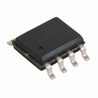
IC CLK ZDB 5OUT 133MHZ 8SOIC

CY23S05SXC-1

Manufacturer Part Number
CY23S05SXC-1
Description
IC CLK ZDB 5OUT 133MHZ 8SOIC
Manufacturer
Cypress Semiconductor Corp
Type
Fanout Distribution, Zero Delay Bufferr
Series
Spread Aware™r
Datasheet

Specifications of CY23S05SXC-1

Number Of Circuits
1
Package / Case
8-SOIC (3.9mm Width)
Pll
Yes
Input
LVCMOS, LVTTL
Output
LVCMOS
Ratio - Input:output
1:5
Differential - Input:output
No/No
Frequency - Max
133.33MHz
Divider/multiplier
No/No
Voltage - Supply
3 V ~ 3.6 V
Operating Temperature
0°C ~ 70°C
Mounting Type
Surface Mount
Frequency-max
133MHz
Output Frequency Range
10 MHz to 133.33 MHz
Supply Voltage (max)
3.6 V
Supply Voltage (min)
3 V
Maximum Operating Temperature
+ 70 C
Minimum Operating Temperature
0 C
Mounting Style
SMD/SMT
Operating Supply Voltage
3.3 V
Lead Free Status / RoHS Status
Lead free / RoHS Compliant
Lead Free Status / RoHS Status
Lead free / RoHS Compliant, Lead free / RoHS Compliant

Available stocks

Company
Part Number
Manufacturer
Quantity
Price
Part Number:
CY23S05SXC-1H
Manufacturer:
CYPRESS
Quantity:
1 535
Part Number:
CY23S05SXC-1HT
Manufacturer:
CYPRESS/赛普拉斯
Quantity:
20 000
Company:
Part Number:
CY23S05SXC-1HT
Quantity:
3 400
Company:
Part Number:
CY23S05SXC-1HT
Quantity:
312
Features
Functional Description
The CY23S09 is a low cost 3.3V zero delay buffer designed to
distribute high speed clocks and is available in a 16-pin SOIC
package. The CY23S05 is an 8-pin version of the CY23S09. It
accepts one reference input, and drives out five low skew clocks.
The -1H versions of each device operate at up to 100 and 133
Cypress Semiconductor Corporation
Document Number: 38-07296 Rev. *F
10 MHz to 100 and 133 MHz Operating Range, compatible
with CPU and PCI bus frequencies
Zero Input-output Propagation Delay
Multiple Low Skew Outputs
Less than 200 ps Cycle-to-cycle jitter is compatible with
Pentium based systems
Test mode to bypass PLL (CY23S09 only, see
Decoding for CY23S09
Available in space saving 16-pin, 150-mil SOIC, 4.4 mm
TSSOP, and 150-mil SSOP (CY23S09) or 8-pin, 150-mil
SOIC package (CY23S05)
3.3V operation, advanced 0.65μ CMOS Technology
Spread Aware
Logic Block Diagram
Output-output skew less than 250 ps
Device-device skew less than 700 ps
One input drives five outputs (CY23S05)
One input drives nine outputs, grouped as 4 + 4 + 1
(CY23S09)
on page 2)
198 Champion Court
Select Input
MHz frequencies and have higher drive than the -1 devices. All
parts have on-chip PLLs that lock to an input clock on the REF
pin. The PLL feedback is on-chip and is obtained from the
CLKOUT pad.
The CY23S09 has two banks of four outputs each, which can be
controlled by the select inputs as shown in the Select Input
Decoding table on
2. If all output clocks are not required, Bank B can be
three-stated. The select inputs also allow the input clock to be
directly applied to the outputs for chip and system testing
purposes.
The CY23S09 and CY23S05 PLLs enter a power down mode
when there are no rising edges on the REF input. In this state,
the outputs are three-stated and the PLL is turned off, resulting
in less than 12.0 μA of current draw (for commercial temperature
devices) and 25.0 μA (for industrial temperature devices). The
CY23S09 PLL shuts down in one additional case, as shown in
the
Multiple CY23S09 and CY23S05 devices can accept the same
input clock and distribute it. In this case, the skew between the
outputs of two devices is guaranteed to be less than 700 ps.
All outputs have less than 200 ps of cycle-to-cycle jitter. The input
to output propagation delay on both devices is guaranteed to be
less than 350 ps; the output to output skew is guaranteed to be
less than 250 ps.
The CY23S05 and CY23S09 is available in two different config-
urations, as shown in the
CY23S05-1 and CY23S09-1 is the base part. The CY23S05-1H
and CY23S09-1H is the high drive version of the -1, and its rise
and fall times are much faster than -1.
Low Cost 3.3V Spread Aware
Select Input Decoding for CY23S09
San Jose
Select Input Decoding for CY23S09
,
CA 95134-1709
Ordering Information
Zero Delay Buffer
CY23S09, CY23S05
Revised March 22, 2010
on page 2.
on page 6. The
408-943-2600
on page
[+] Feedback

Related parts for CY23S05SXC-1

CY23S05SXC-1 Summary of contents

Page 1

... The -1H versions of each device operate 100 and 133 Logic Block Diagram Cypress Semiconductor Corporation Document Number: 38-07296 Rev. *F Low Cost 3.3V Spread Aware MHz frequencies and have higher drive than the -1 devices. All parts have on-chip PLLs that lock to an input clock on the REF pin ...

Page 2

Select Input Decoding for CY23S09 S2 S1 CLOCK A1– Three-state 0 1 Driven 1 0 Driven 1 1 Driven Zero Delay and Skew Control All outputs must be uniformly loaded to achieve Zero Delay between the input and ...

Page 3

Table 1. Pin Description for CY23S09 Pin Signal [2] 1 REF [3] 2 CLKA1 [3] 3 CLKA2 GND [3] 6 CLKB1 [3] 7 CLKB2 [ [ [3] 10 CLKB3 [3] 11 CLKB4 ...

Page 4

Maximum Ratings Supply Voltage to Ground Potential................–0.5V to +7.0V DC Input Voltage (Except REF) ............ –0. Input Voltage REF ............................................. −0. Storage Temperature ................................. –65 Operating Conditions for CY23S05SC-XX and CY23S09SC-XX Parameter V Supply Voltage ...

Page 5

Switching Characteristics for CY23S05SI-1H and CY23S09SI-1H Parameter Description t1 Output Frequency [7] ÷ t Duty Cycle = [7] ÷ t Duty Cycle = [7] t3 Rise Time [7] t Fall Time 4 [7] t ...

Page 6

... CLK out 0.1 μF OUTPUTS V DD 0.1 μF GND GND Ordering Information Ordering Code Package Name Pb-Free CY23S05SXC-1 SZ08 CY23S05SXC-1T SZ08 CY23S05SXC-1H SZ08 CY23S05SXC-1HT SZ08 CY23S05SXI-1 SZ08 CY23S05SXI-1T SZ08 CY23S09SXC-1 SZ16 CY23S09SXC-1T SZ16 CY23S09SXC-1H SZ16 CY23S09SXC-1HT SZ16 CY23S09ZXC-1H ZZ16 CY23S09ZXC-1HT ZZ16 Notes 9 ...

Page 7

Package Diagrams Figure 8. 8-Pin (150-Mil) SOIC S08 and SZ08 Figure 9. 16-Pin (150-Mil) SOIC S16 and SZ16 Document Number: 38-07296 Rev. *F CY23S09, CY23S05 51-85066 *D 51-85068 *C Page [+] Feedback ...

Page 8

Package Diagrams continued Figure 10. 16-Pin TSSOP 4.40 mm Body Z16 and ZZ16 Document Number: 38-07296 Rev. *F CY23S09, CY23S05 51-85091 *B Page [+] Feedback ...

Page 9

... CXQ/PYRS Added device “Status” to Ordering Information KVM Removed obsolete parts from Ordering Information table: CY23S09ZC-1, CY23S09OC-1, CY23S09OC-1H, CY23S09ZXC-1, CY23S09OXC-1, CY23S09OXC-1H. Added CY23S05SXC-1T, CY23S05SXC-1HT, CY23S09SXC-1T, CY23S09SXC-1HT, CY23S09ZXC-1HT. Removed Status column from Ordering Information table; added footnote. Updated package names and added numerical temperature range to Ordering Information table. ...

Page 10

... Cypress against all charges. Any Source Code (software and/or firmware) is owned by Cypress Semiconductor Corporation (Cypress) and is protected by and subject to worldwide patent protection (United States and foreign), United States copyright laws and international treaty provisions. Cypress hereby grants to licensee a personal, non-exclusive, non-transferable license to copy, use, modify, create derivative works of, and compile the Cypress Source Code and derivative works for the sole purpose of creating custom software and or firmware in support of licensee product to be used only in conjunction with a Cypress integrated circuit as specified in the applicable agreement ...

Related keywords