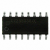
CY25568SXC Cypress Semiconductor Corp, CY25568SXC Datasheet

CY25568SXC
Specifications of CY25568SXC
CY25568SXC
Available stocks
Related parts for CY25568SXC
CY25568SXC Summary of contents
Page 1
... XIN 8pF 16 XOUT 8pF VDD 13 VDD 12 VSS 3 2 VSS Cypress Semiconductor Corporation Document Number: 38-07111 Rev. *C Spread Spectrum Clock Generator Applications ■ Printers and MFPs ■ LCD Panels and Monitors ■ Digital Copiers ■ PDAs ■ Automotive ■ CD-ROM, VCD and DVD ■ ...
Page 2
Pinouts Pin Definitions Pin Function 1 Xin/CLK Clock, crystal or ceramic resonator input pin. 2 VSS Power Supply Ground. 3 VSS Power Supply Ground Digital Spread % control pin. 3-Level input (H-M-L). Default= Digital Spread % ...
Page 3
Absolute Maximum Ratings [1] Exceeding maximum ratings may shorten the useful life of the device. User guidelines are not tested. Supply Voltage (VDD): ................................................. +5.5V Input Voltage Relative to VDD: ............................ VDD+0.3V Note : Operation at any Absolute Maximum Rating ...
Page 4
Input Frequency Range and Selection The CY25568 input frequency range MHz. This range is divided into 3 segments and controlled by 3-Level FRSEL pin as given in Table 1. Table 1. Input Frequency Selection FRSEL INPUT ...
Page 5
Spread % Selection The CY25568 provides Center-Spread, Down-Spread and No-Spread functions. These functions and the amount of Spread % are selected by using 3-Level S0 and S1 digital inputs and are given in Table 3. Spread % Selection XIN S1=0 ...
Page 6
Power Down (PD#) CY25568 includes a Power Down (PD#, Pin 10) function. This input uses standard 2-Level CMOS logic and is internally pulled up to VDD (HIGH). Connect this pin to GND if power turned off. Modulation ...
Page 7
Characteristic Curves The following curves demonstrate the characteristic behavior of the CY25568 when tested over a number of environmental and application specific parameters. These are typical performance curves and are not meant to replace any parameter specified in tables “DC ...
Page 8
SSCG Profiles The CY25568 uses a non-linear frequency profile as shown in maintains flat energy distribution over the fundamental and higher order harmonics. This results in additional EMI reduction in electronic systems. Figure 7. Spread Spectrum Profiles (Frequency versus Time) ...
Page 9
... Application Schematic Ordering Information Part No. Pb-Free CY25568SXC CY25568SXCT Document Number: 38-07111 Rev. *C Figure 8. Application Schematic Package 16 Pin SOIC 16 Pin SOIC – Tape and Reel CY25568 Operating Temperature Range 0 to 70° 70°C Page [+] Feedback ...
Page 10
Package Diagram Document Number: 38-07111 Rev. *C Figure 9. 16-Pin (150-Mil) SOIC CY25568 51-85068 *B Page [+] Feedback ...
Page 11
... Cypress against all charges. Any Source Code (software and/or firmware) is owned by Cypress Semiconductor Corporation (Cypress) and is protected by and subject to worldwide patent protection (United States and foreign), United States copyright laws and international treaty provisions. Cypress hereby grants to licensee a personal, non-exclusive, non-transferable license to copy, use, modify, create derivative works of, and compile the Cypress Source Code and derivative works for the sole purpose of creating custom software and or firmware in support of licensee product to be used only in conjunction with a Cypress integrated circuit as specified in the applicable agreement ...


