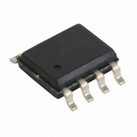
CY25560SXC Cypress Semiconductor Corp, CY25560SXC Datasheet

CY25560SXC
Specifications of CY25560SXC
CY25560SXC
Available stocks
Related parts for CY25560SXC
CY25560SXC Summary of contents
Page 1
... Commercial and Industrial Temperature Ranges Logic Block Diagram Xin/ 1 CLK Xout 8 VDD 2 3 VSS Cypress Semiconductor Corporation Document #: 38-07425 Rev. *F Spread Spectrum Clock Generator Applications ■ Desktop, Notebook, and Tablet PCs ■ VGA Controllers ■ LCD Panels and Monitors ■ Printers and Multifunction Devices (MFP) Benefits ■ ...
Page 2
Pinouts Figure 1. Pin Configuration – 8-Pin SOIC Package Table 1. Pin Description Pin Number Pin Name Type 1 Xin/CLK I Clock or Crystal Connection Input. Refer to 2 VDD P Positive Power Supply. 3 GND P Power Supply Ground. ...
Page 3
CY25560 "M" (N/ "0" (GND) VDD 5 SSCC = "1" Table 2. Frequency and Spread% Selection Input S1=M Frequency S0=M (MHz) 25 – – – – ...
Page 4
SSCG SSCG uses a patented technology of modulating the clock over a very narrow bandwidth and controlled rate of change, both peak and cycle-to-cycle. The CY25560 takes a narrow band digital reference clock in the range 100 ...
Page 5
CY25560 Application Schematic The schematic in Figure 4 demonstrates how the CY25560 is configured in a typical application. This application is shown as using a 30 MHz fundamental crystal. In most applications, an external reference clock is used. Apply the ...
Page 6
Absolute Maximum Ratings [1, 2] Commercial Grade Supply Voltage (V ):.....................................–0.5V to +6. Input Voltage: ................................... –0.5V to VDD+0.5V Junction Temperature ................................. –40°C to +140°C Operating Temperature:...................................... 0°C to 70°C Storage Temperature .................................. –65°C to +150°C Static Discharge ...
Page 7
... R D Input Clock Duty Cycle TYin D Output Clock Duty Cycle TYout J Cycle-to-Cycle Jitter CC1 J Cycle-to-Cycle Jitter CC2 Ordering Information Part Number Pb-Free CY25560SXC CY25560SXCT CY25560SXI CY25560SXIT Document #: 38-07425 Rev. *F (Pin pF, Unless Otherwise Noted L Conditions ±10% S0 and S1 only S0 and S1 only S0 and S1 only ...
Page 8
Package Drawing and Dimensions Document #: 38-07425 Rev. *F Figure 5. 8-Pin (150-Mil) SOIC S8 CY25560 51-85066-*C Page [+] Feedback ...
Page 9
... Cypress against all charges. Any Source Code (software and/or firmware) is owned by Cypress Semiconductor Corporation (Cypress) and is protected by and subject to worldwide patent protection (United States and foreign), United States copyright laws and international treaty provisions. Cypress hereby grants to licensee a personal, non-exclusive, non-transferable license to copy, use, modify, create derivative works of, and compile the Cypress Source Code and derivative works for the sole purpose of creating custom software and or firmware in support of licensee product to be used only in conjunction with a Cypress integrated circuit as specified in the applicable agreement ...


