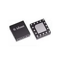
BGA 748L16 E6327 Infineon Technologies, BGA 748L16 E6327 Datasheet
BGA 748L16 E6327
Specifications of BGA 748L16 E6327


Related parts for BGA 748L16 E6327

BGA 748L16 E6327 Summary of contents
Page 1
High Linearity Quad-Band UMTS LNA (2100, 1900, 900, 800 MHz Revision 3.0, 2010-11- & ...
Page 2
... Infineon Technologies Office. Infineon Technologies components may be used in life-support devices or systems only with the express written approval of Infineon Technologies failure of such components can reasonably be expected to cause the failure of that life-support device or system or to affect the safety or effectiveness of that device or system. Life support devices or systems are intended to be implanted in the human body or to support and/or maintain and sustain and/or protect human life ...
Page 3
... Page Subjects (major changes since last revision) Trademarks of Infineon Technologies AG AURIX™, BlueMoon™, C166™, CanPAK™, CIPOS™, CIPURSE™, COMNEON™, EconoPACK™, CoolMOS™, CoolSET™, CORECONTROL™, CROSSAVE™, DAVE™, EasyPIM™, EconoBRIDGE™, EconoDUAL™, EconoPIM™ ...
Page 4
Table of Contents Table of Contents . . . . . . . . . . . . . . . . . . . . . . . . . . . . . . . . . . ...
Page 5
List of Figures Figure 1 Block Diagram of Quad-Band LNA . . . . . . . . . . . . . . . . . . . . . . . . . . . . . . ...
Page 6
List of Tables Table 1 Absolute Maximum Ratings . . . . . . . . . . . . . . . . . . . . . . . . . . . . . . . . ...
Page 7
High Linearity Quad-Band UMTS LNA (2100, 1900, 900, 800 MHz) 1 Features Main features: • Gain typ. in high / low gain mode (all bands) • Noise figure: 1.1 dB typ. in high gain mode • ...
Page 8
Figure 1 Block Diagram of Quad-Band LNA Data Sheet High Linearity Quad-Band UMTS LNA 8 Revision 3.0, 2010-11-08 BGA748N16 Features ...
Page 9
Electrical Characteristics 2.1 Absolute Maximum Ratings Table 1 Absolute Maximum Ratings Parameter Supply voltage Supply current Pin voltage Pin voltage RF Input Pins RF input power Junction temperature Ambient temperature range Storage temperature range Attention: Stresses exceeding the max. ...
Page 10
DC Characteristics Table 4 DC Characteristics, Parameter Symbol V Supply voltage CC I Supply current high gain CCHG mode I Supply current low gain CCLG mode I Supply current standby CCOFF mode V Logic level high HI V Logic ...
Page 11
Supply Current Characteristics Supply current high gain mode versus resistance of reference resistor R low gain mode supply current is independent of reference resistor). I Supply Current Band 2 ...
Page 12
Logic Signal Characteristics Current consumption of logic inputs VEN1, VEN2, VGS, VON I V Logic currents = f( ) LOG LOG ° ...
Page 13
Measured RF Characteristics UMTS Band V Table 8 Typical Characteristics 880 MHz Band, Parameter Pass band range Current consumption Gain 2) Reverse Isolation Noise figure 2) Input return loss 2) Output return loss 3) Stability factor 2) Input compression ...
Page 14
Measured RF Characteristics UMTS Band V Table 9 Typical Characteristics 880 MHz Band, Parameter Pass band range Current consumption Gain 2) Reverse Isolation Noise figure 2) Input return loss 2) Output return loss 3) Stability factor 2) Input compression ...
Page 15
Measured RF Characteristics UMTS Band V Table 10 Typical Characteristics 880 MHz Band, Parameter Pass band range Current consumption Gain 2) Reverse Isolation Noise figure 2) Input return loss 2) Output return loss 3) Stability factor 2) Input compression ...
Page 16
Measured RF Characteristics UMTS Band VIII Table 11 Typical Characteristics 940 MHz Band, Parameter Pass band range Current consumption Gain 2) Reverse Isolation Noise figure 2) Input return loss 2) Output return loss 3) Stability factor 2) Input compression ...
Page 17
Measured RF Characteristics UMTS Band VIII Table 12 Typical Characteristics 940 MHz Band, Parameter Pass band range Current consumption Gain 2) Reverse Isolation Noise figure 2) Input return loss 2) Output return loss 3) Stability factor 2) Input compression ...
Page 18
Measured RF Characteristics UMTS Band VIII Table 13 Typical Characteristics 940 MHz Band, Parameter Pass band range Current consumption Gain 2) Reverse Isolation Noise figure 2) Input return loss 2) Output return loss 3) Stability factor 2) Input compression ...
Page 19
Measured RF Characteristics UMTS Band II Table 14 Typical Characteristics 1960 MHz Band, Parameter Pass band range Current consumption Gain 2) Reverse Isolation Noise figure 2) Input return loss 2) Output return loss 3) Stability factor 2) Input compression ...
Page 20
Measured RF Characteristics UMTS Band II Table 15 Typical Characteristics 1960 MHz Band, Parameter Pass band range Current consumption Gain 2) Reverse Isolation Noise figure 2) Input return loss 2) Output return loss 3) Stability factor 2) Input compression ...
Page 21
Measured RF Characteristics UMTS Band II Table 16 Typical Characteristics 1960 MHz Band, Parameter Pass band range Current consumption Gain 2) Reverse Isolation Noise figure 2) Input return loss 2) Output return loss 3) Stability factor 2) Input compression ...
Page 22
Measured RF Characteristics UMTS Band I Table 17 Typical Characteristics 2140 MHz Band, Parameter Pass band range Current consumption Gain 2) Reverse Isolation Noise figure 2) Input return loss 2) Output return loss 3) Stability factor 2) Input compression ...
Page 23
Measured RF Characteristics UMTS Band I Table 18 Typical Characteristics 2140 MHz Band, Parameter Pass band range Current consumption Gain 2) Reverse Isolation Noise figure 2) Input return loss 2) Output return loss 3) Stability factor 2) Input compression ...
Page 24
Measured RF Characteristics UMTS Band I Table 19 Typical Characteristics 2140 MHz Band, Parameter Pass band range Current consumption Gain 2) Reverse Isolation Noise figure 2) Input return loss 2) Output return loss 3) Stability factor 2) Input compression ...
Page 25
Application Circuit and Block Diagram 3.1 UMTS Bands I, II, V and VIII Application Circuit Schematic C1 1.8pF RFIN Band II C3 10pF RFIN Band I 2.2nH C5 2.4pF RFIN Band V RFIN Band VIII Figure 2 Application Circuit ...
Page 26
Pin Description Table 21 Pin Definition and Function Pin No. Name 0 GND 1 RFOUT8 2 RFOUT5 3 RFOUT1 4 RFOUT2 5 RREF 6 VGS 7 VCC 8 RFGND1 9 VON 10 RFIN2 11 RFIN1 12 RFGND2 13 RFIN5 ...
Page 27
Application Board Note: Top layer thickness: 0.2 mm, bottom layer thickness: 0.8 mm metallization, gold plated. Board size 45mm. Figure 3 Cross-Section View of Application Board Data Sheet High Linearity Quad-Band UMTS LNA Application ...
Page 28
Figure 4 Detail of Application Board Layout Note: In order to achieve the same performance as given in this datasheet please follow the suggested PCB-layout as closely as possible. The position of the GND vias is critical for RF performance. ...
Page 29
Physical Characteristics 4.1 Package Footprint Figure 5 Recommended Footprint and Stencil Layout for the TSNP-16-1 Package Data Sheet High Linearity Quad-Band UMTS LNA Physical Characteristics 29 BGA748N16 Revision 3.0, 2010-11-08 ...
Page 30
Package Dimensions Figure 6 Package Outline (Top, Side and Bottom View) Data Sheet High Linearity Quad-Band UMTS LNA Physical Characteristics 30 BGA748N16 Revision 3.0, 2010-11-08 ...
Page 31
... Published by Infineon Technologies AG ...