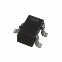
BFS25A,115 NXP Semiconductors, BFS25A,115 Datasheet - Page 3

BFS25A,115
Manufacturer Part Number
BFS25A,115
Description
TRANS NPN 5V 6.5MA SOT323
Manufacturer
NXP Semiconductors
Datasheet
1.BFS25A115.pdf
(13 pages)
Specifications of BFS25A,115
Package / Case
SC-70-3, SOT-323-3
Transistor Type
NPN
Voltage - Collector Emitter Breakdown (max)
5V
Frequency - Transition
5GHz
Noise Figure (db Typ @ F)
1.8dB ~ 2dB @ 1GHz
Power - Max
32mW
Dc Current Gain (hfe) (min) @ Ic, Vce
50 @ 500µA, 1V
Current - Collector (ic) (max)
6.5mA
Mounting Type
Surface Mount
Dc Collector/base Gain Hfe Min
50
Dc Current Gain Hfe Max
50 @ 0.5mA @ 1V
Minimum Operating Temperature
- 65 C
Mounting Style
SMD/SMT
Configuration
Single
Transistor Polarity
NPN
Maximum Operating Frequency
5000 MHz (Typ)
Collector- Emitter Voltage Vceo Max
5 V
Emitter- Base Voltage Vebo
2 V
Continuous Collector Current
6.5 mA
Power Dissipation
32 mW
Maximum Operating Temperature
+ 175 C
Lead Free Status / RoHS Status
Lead free / RoHS Compliant
Gain
-
Lead Free Status / Rohs Status
Lead free / RoHS Compliant
Other names
934021360115
BFS25A T/R
BFS25A T/R
BFS25A T/R
BFS25A T/R
Available stocks
Company
Part Number
Manufacturer
Quantity
Price
Part Number:
BFS25A,115
Manufacturer:
NXP/恩智浦
Quantity:
20 000
NXP Semiconductors
THERMAL RESISTANCE
Note
1. T
CHARACTERISTICS
T
Note
1. G
December 1997
R
I
h
C
f
G
F
SYMBOL
j
CBO
T
FE
= 25 C, unless otherwise specified.
NPN 5 GHz wideband transistor
th j-s
re
SYMBOL
UM
G
s
UM
is the temperature at the soldering point of the collector tab.
UM
is the maximum unilateral power gain, assuming S
=
collector cut-off current
DC current gain
feedback capacitance
transition frequency
maximum unilateral power
gain (note 1)
noise figure
10 log
thermal resistance from junction to
soldering point
PARAMETER
--------------------------------------------------------- - dB.
1
–
S
11
PARAMETER
S
2
1
21
2
–
S
22
2
I
I
I
I
T
I
T
T
f = 1 GHz; T
E
C
C
C
C
amb
amb
s
amb
s
= 0; V
= 0.5 mA; V
= 0; V
= 1 mA; V
= 0.5 mA; V
=
=
= 25 C
= 25 C
= 25 C
opt
opt
CB
CB
; I
; I
C
C
= 5 V
= 1 V; f = 1 MHz
= 0.5 mA; V
= 1 mA; V
amb
CE
CE
CE
= 1 V; f = 1 GHz;
CONDITIONS
up to T
= 25 C
3
= 1 V
= 1 V; f = 1 GHz;
12
is zero and
CE
s
CONDITIONS
CE
= 170 C; note 1
= 1 V;
= 1 V; f = 1 GHz;
50
3.5
MIN.
THERMAL RESISTANCE
80
0.3
5
13
1.8
2
TYP.
Product specification
190 K/W
BFS25A
50
200
0.45
MAX.
nA
pF
GHz
dB
dB
dB
UNIT


