MRF1518NT1 Freescale Semiconductor, MRF1518NT1 Datasheet - Page 16
MRF1518NT1
Manufacturer Part Number
MRF1518NT1
Description
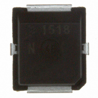
IC MOSFET RF N-CHAN PLD-1.5
Manufacturer
Freescale Semiconductor
Datasheet
1.MRF1518NT1.pdf
(19 pages)
Specifications of MRF1518NT1
Transistor Type
N-Channel
Frequency
520MHz
Gain
13dB
Voltage - Rated
40V
Current Rating
4A
Current - Test
150mA
Voltage - Test
12.5V
Power - Output
8W
Package / Case
PLD-1.5
Configuration
Single Dual Source
Drain-source Breakdown Voltage
40 V
Gate-source Breakdown Voltage
+/- 20 V
Continuous Drain Current
4 A
Power Dissipation
62500 mW
Maximum Operating Temperature
+ 150 C
Minimum Operating Temperature
- 65 C
Mounting Style
SMD/SMT
Transistor Polarity
N-Channel
Drain Source Voltage Vds
40V
Continuous Drain Current Id
4mA
Power Dissipation Pd
62.5W
Rf Transistor Case
PLD-1.5
Termination Type
SMD
Output Power Pout
8W
Rohs Compliant
Yes
Filter Terminals
SMD
Gate-source Voltage
20V
Lead Free Status / RoHS Status
Contains lead / RoHS non-compliant
Noise Figure
-
Lead Free Status / Rohs Status
Lead free / RoHS Compliant
Other names
MRF1518NT1
MRF1518NT1TR
MRF1518NT1TR
Available stocks
Company
Part Number
Manufacturer
Quantity
Price
Company:

Part Number:
MRF1518NT1
Manufacturer:
FREESCALE
Quantity:
1 400


MOUNTING
sumes a majority of the 0.065″ x 0.180″ source contact on
the back side of the package is in good contact with an ap-
propriate heat sink. As with all RF power devices, the goal of
the thermal design should be to minimize the temperature at
the back side of the package. Refer to Freescale Application
Note AN4005/D, “Thermal Management and Mounting Meth-
od for the PLD - 1.5 RF Power Surface Mount Package,” and
Engineering Bulletin EB209/D, “Mounting Method for RF
Power Leadless Surface Mount Transistor” for additional in-
formation.
AMPLIFIER DESIGN
bipolar transistors are suitable for this device. For examples
see Freescale Application Note AN721, “Impedance
Matching Networks Applied to RF Power Transistors.”
MRF1518NT1
16
The specified maximum thermal resistance of 2°C/W as-
Impedance matching networks similar to those used with
Large - signal impedances are provided, and will yield a good
first pass approximation.
unilateral. This coupled with the very high gain of this device
yields a device capable of self oscillation. Stability may be
achieved by techniques such as drain loading, input shunt
resistive loading, or output to input feedback. The RF test fix-
ture implements a parallel resistor and capacitor in series
with the gate, and has a load line selected for a higher effi-
ciency, lower gain, and more stable operating region.
S - parameters provides a useful tool for selection of loading
or feedback circuitry to assure stable operation. See Free-
scale Application Note AN215A, “RF Small - Signal Design
Using Two - Port Parameters” for a discussion of two port
network theory and stability.
Since RF power MOSFETs are triode devices, they are not
Two - port stability analysis with this device’s
Freescale Semiconductor
RF Device Data
Related parts for MRF1518NT1
Image
Part Number
Description
Manufacturer
Datasheet
Request
R

Part Number:
Description:
MRF1518RF Power Field Effect Transistor
Manufacturer:
Freescale Semiconductor, Inc


Part Number:
Description:
Fast Acting Radial Lead Micro Fuse Series
Manufacturer:
BEL [Bel Fuse Inc.]
Datasheet:

Part Number:
Description:
FUSE 1A 250V FAST SHORT MRF
Manufacturer:
Bel Fuse Inc
Datasheet:
Part Number:
Description:
Manufacturer:
Freescale Semiconductor, Inc
Datasheet:
Part Number:
Description:
Manufacturer:
Freescale Semiconductor, Inc
Datasheet:
Part Number:
Description:
Manufacturer:
Freescale Semiconductor, Inc
Datasheet:
Part Number:
Description:
Manufacturer:
Freescale Semiconductor, Inc
Datasheet:
Part Number:
Description:
Manufacturer:
Freescale Semiconductor, Inc
Datasheet:
Part Number:
Description:
Manufacturer:
Freescale Semiconductor, Inc
Datasheet:
Part Number:
Description:
Manufacturer:
Freescale Semiconductor, Inc
Datasheet:
Part Number:
Description:
Manufacturer:
Freescale Semiconductor, Inc
Datasheet:
Part Number:
Description:
Manufacturer:
Freescale Semiconductor, Inc
Datasheet:
Part Number:
Description:
Manufacturer:
Freescale Semiconductor, Inc
Datasheet:
Part Number:
Description:
Manufacturer:
Freescale Semiconductor, Inc
Datasheet: