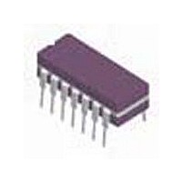
8601401CA National Semiconductor, 8601401CA Datasheet - Page 11

8601401CA
Manufacturer Part Number
8601401CA
Description
Comparator Dual ±18V/36V 14-Pin CDIP Rail
Manufacturer
National Semiconductor
Datasheet
1.8601401CA.pdf
(20 pages)
Specifications of 8601401CA
Package
14CDIP
Typical Response Time
0.08 us
Typical Response Time Range
0.05 to 0.5 us
Output Type
Open Collector
Number Of Channels Per Chip
2
Minimum Single Supply Voltage
5 V
Power Supply Type
Single|Dual
Number Of Elements
2
Technology
Bipolar
Input Offset Voltage
3.8@5VmV
Input Bias Current (typ)
150pA
Input Voltage Range
-13/13V
Response Time
80ns
Single Supply Voltage (typ)
9/12/15/18/24/28V
Dual Supply Voltage (typ)
Not RequiredV
Supply Current (max)
11@±15VmA
Common Mode Rejection Ratio
80dB
Voltage Gain In Db
92.04dB
Power Supply Requirement
Single/Dual
Single Supply Voltage (min)
5V
Single Supply Voltage (max)
36V
Dual Supply Voltage (min)
±2.5V
Dual Supply Voltage (max)
±18V
Power Dissipation
500mW
Operating Temp Range
-55C to 125C
Operating Temperature Classification
Military
Mounting
Through Hole
Pin Count
14
Package Type
CDIP
Lead Free Status / Rohs Status
Not Compliant
Available stocks
Company
Part Number
Manufacturer
Quantity
Price
+I
-I
V
I
V
IB
CC
IO
IO
Symbol
Symbol
CC
SMD 5962-9679802, ELDRS FREE DC DELTA Parameters
The following conditions apply, unless otherwise specified.
SMD 5962-9679802, ELDRS FREE 100K Post Radiation Parameters @ 25°C
The following conditions apply, unless otherwise specified. V
Note 2: Absolute Maximum Ratings indicate limits beyond which damage to the device may occur. Operating Ratings indicate conditions for which the device is
functional, but do not guarantee specific performance limits. For guaranteed specifications and test conditions, see the Electrical Characteristics. The guaranteed
specifications apply only for the test conditions listed. Some performance characteristics may degrade when the device is not operated under the listed test
conditions.
Note 3: The maximum power dissipation must be derated at elevated temperatures and is dictated by T
junction to ambient thermal resistance), and T
θ
Note 4: For supply voltages less than ±15V the absolute maximum input voltage is equal to the supply voltage.
Note 5: Human Body model, 1.5KΩ in series with 100pF.
Note 6: V
Note 7: 5V differential across +V
Note 8: Parameter guaranteed by V
Note 9: K = V/mV.
Note 10: Gain is computed with an output swing from +13.5V to +1.5V.
Note 11: Gain is computed with an output swing from +5.0V to +0.5V.
Note 12: Output is monitored by measuring V
Note 13: Pre and post irradiation limits are identical to those listed under AC and DC electrical characteristics except as listed in the Post Radiation Limits Table.
These parts may be dose rate sensitive in a space environment and demonstrate enhanced low dose rate sensitivity. Radiation end point limits for the noted
parameters are guaranteed only for the conditions as specified in MIL-STD-883, per Test Method 1019, Condition A.
Note 14: Pre and post irradiation limits are identical to those listed under AC and DC electrical characteristics except as listed in the Post Radiation Limits Table.
Low dose rate testing has been performed on a wafer-by-wafer basis, per Test Method 1019, Condition D of MIL-STD-883, with no enhanced low dose rate
sensitivity (ELDRS).
(Note 14)
JA
V
or the number given in the Absolute Maximum Ratings, whichever is lower.
CM
= 0V, Delta calculations performed on QMLV devices at group B, subgroup 5 only.
I
≥
8mV at extremes for I
Positive Supply Current
Negative Supply Current
Input Offset Voltage
Input Bias Current
Input Offset Voltage
Parameter
Parameter
CC
Leak
and −V
IO
and I
and V
CC
IO
I
.
I
A
tests.
≤
with limits from 0 to 6mV at all temperatures
(ambient temperature). The maximum allowable power dissipation at any temperature is P
−8mV at extremes for V
±V
V
±V
V
+
±V
V
+
+
±V
5KΩ
±V
5KΩ
V
V
V
+
+
CC
CC
CC
CC
CC
CC
CC
CC
CC
= 5.6V thru 1.4KΩ
= 5.6V thru 1.4KΩ
= 5V
= 5V, V
= 5V, V
= 5V, V
= ±15V, V
= ±15V, V
= ±15V
= ±15V, V
= ±15V, V
Conditions
Conditions
CM
CM
CM
Sat
O
O
CM
CM
(V
= 1V, R
= 1V, R
= 3V, R
CM
= Low
= Low
I
11
to exceed V
= 12V, R
= −12V, R
= 0V
S
S
S
≤
≤
≤
5KΩ
5KΩ
5KΩ
S
OS
S
≤
.
≤
Notes
Notes
Jmax
(maximum junction temperature), θ
Min
-1.0
-0.5
-0.4
Min
-4.0
-4.0
-4.0
-4.0
Max
Max
1.0
0.5
0.4
1.0
1.0
4.0
4.0
4.0
4.0
Units
Units
mA
mA
mV
mV
mV
mV
mV
µA
µA
Dmax
= (T
JA
www.national.com
(package
Jmax
groups
groups
- T
Sub-
Sub-
1
1
1
1
1
1
1
1
1
A
)/


