STW45NM50FD STMicroelectronics, STW45NM50FD Datasheet
STW45NM50FD
Specifications of STW45NM50FD
Available stocks


Related parts for STW45NM50FD


STW45NM50FD Summary of contents
Page 1
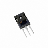
... Table 1. Device summary Order code STW45NM50FD July 2009 N-channel 500 V, 0.07 Ω TO-247 FDmesh™ Power MOSFET (with fast diode) R DS(on max < 0.1 Ω Figure 1. Marking Package W45NM50FD Doc ID 7955 Rev 10 STW45NM50FD TO-247 Internal schematic diagram Packaging TO-247 Tube 1/12 www.st.com 12 ...
Page 2
... Contents Contents 1 Electrical ratings . . . . . . . . . . . . . . . . . . . . . . . . . . . . . . . . . . . . . . . . . . . . 3 2 Electrical characteristics . . . . . . . . . . . . . . . . . . . . . . . . . . . . . . . . . . . . . 4 2.1 Electrical characteristics (curves) 3 Test circuits 4 Package mechanical data . . . . . . . . . . . . . . . . . . . . . . . . . . . . . . . . . . . . . 9 5 Revision history . . . . . . . . . . . . . . . . . . . . . . . . . . . . . . . . . . . . . . . . . . . 11 2/ Doc ID 7955 Rev 10 STW45NM50FD ...
Page 3
... STW45NM50FD 1 Electrical ratings Table 2. Absolute maximum ratings Symbol V Drain-source voltage ( Gate-source voltage GS I Drain current (continuous Drain current (continuous (1) I Drain current (pulsed Total dissipation at T TOT Derating factor (2) dv/dt Peak diode recovery voltage slope T Operating junction temperature J T Storage temperature stg 1 ...
Page 4
... Parameter Test conditions V >I DS D(on 22 =25 V, f=1 MHz = 400 = Figure 14 f=1 MHz Gate DC Bias= 0 test signal level = 20 mV open drain DSS Doc ID 7955 Rev 10 STW45NM50FD Min. Typ 500 GS = 250 µ 22.5 A 0.07 D Min. Typ DS(on)max - 20 3600 =0 - 1260 400 V - 350 = oss Max. ...
Page 5
... STW45NM50FD Table 7. Switching times Symbol t Turn-on delay time d(on) t Rise time r t Off-voltage rise time r(Voff) t Fall time f t Cross-over time c Table 8. Source drain diode Symbol I Source-drain current SD (1) I Source-drain current (pulsed) SDM (2) V Forward on voltage SD t Reverse recovery time rr Q Reverse recovery charge ...
Page 6
... Electrical characteristics 2.1 Electrical characteristics (curves) Figure 2. Safe operating area Figure 4. Output characteristics Figure 6. Transconductance 6/12 Figure 3. Thermal impedance Figure 5. Transfer characteristics Figure 7. Static drain-source on resistance Doc ID 7955 Rev 10 STW45NM50FD ...
Page 7
... STW45NM50FD Figure 8. Gate charge vs gate-source voltage Figure 9. Figure 10. Normalized gate threshold voltage vs temperature Figure 12. Source-drain diode forward characteristics Capacitance variations Figure 11. Normalized on resistance vs temperature Doc ID 7955 Rev 10 Electrical characteristics 7/12 ...
Page 8
... AM01468v1 Figure 16. Unclamped inductive load test 3.3 1000 µF µ AM01470v1 Figure 18. Switching time waveform V (BR)DSS 10% 0 AM01472v1 Doc ID 7955 Rev 10 STW45NM50FD 12V 47kΩ 100nF I =CONST G 100Ω GMAX 2200 µF 2.7kΩ 47kΩ 1kΩ circuit 2200 3.3 µ ...
Page 9
... STW45NM50FD 4 Package mechanical data In order to meet environmental requirements, ST offers these devices in different grades of ® ECOPACK packages, depending on their level of environmental compliance. ECOPACK specifications, grade definitions and product status are available at: www.st.com. ECOPACK trademark. Doc ID 7955 Rev 10 Package mechanical data ® 9/12 ...
Page 10
... Package mechanical data Dim ø P ø 10/12 TO-247 Mechanical data mm. Min. Typ Doc ID 7955 Rev 10 STW45NM50FD Max ...
Page 11
... STW45NM50FD 5 Revision history Table 9. Document revision history Date 05-Apr-2005 26-Apr-2006 23-Jul-2009 Revision Source drain diode 8 Modified value on 9 New template Switching times 10 Modified values on Doc ID 7955 Rev 10 Revision history Changes 11/12 ...
Page 12
... Australia - Belgium - Brazil - Canada - China - Czech Republic - Finland - France - Germany - Hong Kong - India - Israel - Italy - Japan - Malaysia - Malta - Morocco - Philippines - Singapore - Spain - Sweden - Switzerland - United Kingdom - United States of America 12/12 Please Read Carefully: © 2009 STMicroelectronics - All rights reserved STMicroelectronics group of companies www.st.com Doc ID 7955 Rev 10 STW45NM50FD ...