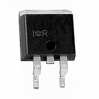
IRL8113SPBF International Rectifier, IRL8113SPBF Datasheet - Page 6

IRL8113SPBF
Manufacturer Part Number
IRL8113SPBF
Description
MOSFET N-CH 30V 105A D2PAK
Manufacturer
International Rectifier
Series
HEXFET®r
Datasheet
1.IRL8113LPBF.pdf
(13 pages)
Specifications of IRL8113SPBF
Fet Type
MOSFET N-Channel, Metal Oxide
Fet Feature
Logic Level Gate
Rds On (max) @ Id, Vgs
6 mOhm @ 21A, 10V
Drain To Source Voltage (vdss)
30V
Current - Continuous Drain (id) @ 25° C
105A
Vgs(th) (max) @ Id
2.25V @ 250µA
Gate Charge (qg) @ Vgs
35nC @ 4.5V
Input Capacitance (ciss) @ Vds
2840pF @ 15V
Power - Max
110W
Mounting Type
Surface Mount
Package / Case
D²Pak, TO-263 (2 leads + tab)
Transistor Polarity
N Channel
Continuous Drain Current Id
105A
Drain Source Voltage Vds
30V
On Resistance Rds(on)
6mohm
Rds(on) Test Voltage Vgs
10V
Peak Reflow Compatible (260 C)
Yes
Rohs Compliant
Yes
Resistance Drain-source Rds (on)
7.1 mOhms
Drain-source Breakdown Voltage
30 V
Gate-source Breakdown Voltage
20 V
Continuous Drain Current
105 A
Power Dissipation
110 W
Mounting Style
SMD/SMT
Gate Charge Qg
23 nC
Lead Free Status / RoHS Status
Lead free / RoHS Compliant
Other names
*IRL8113SPBF
6
Fig 13a. Unclamped Inductive Test Circuit
Fig 13b. Unclamped Inductive Waveforms
Fig 12. On-Resistance Vs. Gate Voltage
40
30
20
10
0
I
2.0
AS
R G
20V
V
V DS
GS
V GS , Gate-to-Source Voltage (V)
t p
4.0
I AS
D.U.T
t p
0.01 Ω
L
6.0
T J = 125°C
T J = 25°C
15V
V
8.0
(BR)DSS
DRIVER
I D = 21A
+
-
V DD
10.0
A
1000
800
600
400
200
90%
V
0
10%
V
DS
Fig 14b. Switching Time Waveforms
Fig 14a. Switching Time Test Circuit
25
GS
Fig 13c. Maximum Avalanche Energy
Starting T J , Junction Temperature (°C)
t
50
d(on)
Duty Factor < 0.1%
Pulse Width < 1µs
Vs. Drain Current
V
GS
t
75
r
V
DS
100
t
d(off)
125
TOP
BOTTOM
www.irf.com
D.U.T
L
t
D
f
V
150
DD
11A
8.8A
I D
17A
+
-
175


