PHB45NQ10T,118 NXP Semiconductors, PHB45NQ10T,118 Datasheet
PHB45NQ10T,118
Specifications of PHB45NQ10T,118
Available stocks


Related parts for PHB45NQ10T,118


PHB45NQ10T,118 Summary of contents
Page 1
PHB45NQ10T N-channel TrenchMOS standard level FET Rev. 02 — 8 July 2010 1. Product profile 1.1 General description Standard level N-channel enhancement mode Field-Effect Transistor (FET plastic package using TrenchMOS technology. This product is designed and qualified for ...
Page 2
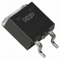
... NXP Semiconductors 2. Pinning information Table 2. Pinning information Pin Symbol Description 1 G gate [ drain 3 S source mb D mounting base; connected to drain [ not possible to make connection to pin 2. 3. Ordering information Table 3. Ordering information Type number Package Name PHB45NQ10T D2PAK PHB45NQ10T Product data sheet ...
Page 3
... NXP Semiconductors 4. Limiting values Table 4. Limiting values In accordance with the Absolute Maximum Rating System (IEC 60134). Symbol Parameter V drain-source voltage DS V drain-gate voltage DGR V gate-source voltage GS I drain current D I peak drain current DM P total power dissipation tot T storage temperature stg ...
Page 4
... NXP Semiconductors DSon − ° single pulse mb DM Fig 3. Safe operating area; continuous and peak drain currents as a function of drain-source voltage 5. Thermal characteristics Table 5. Thermal characteristics Symbol Parameter R thermal resistance th(j-mb) from junction to mounting base R thermal resistance th(j-a) from junction to ambient Fig 5 ...
Page 5
... NXP Semiconductors 6. Characteristics Table 6. Characteristics Symbol Parameter Static characteristics V drain-source (BR)DSS breakdown voltage V gate-source threshold GS(th) voltage I drain leakage current DSS I gate leakage current GSS R drain-source on-state DSon resistance Dynamic characteristics Q total gate charge G(tot) Q gate-source charge GS Q gate-drain charge GD C input capacitance ...
Page 6
... NXP Semiconductors ( 0.4 0 °C j Fig 6. Output characteristics: drain current as a function of drain-source voltage; typical values ( 175 ° > DSon Fig 8. Transfer characteristics: drain current as a function of gate-source voltage; typical values 2.9 a 2.1 1.3 0.5 −60 20 Fig 10. Normalized drain-source on-state resistance factor as a function of junction temperature ...
Page 7
... NXP Semiconductors − (A) −2 10 −3 10 minimum −4 10 −5 10 − ° Fig 12. Sub-threshold drain current as a function of gate-source voltage ( ° Fig 14. Gate-source voltage as a function of gate charge; typical values PHB45NQ10T Product data sheet 014aab212 typical maximum (V) GS Fig 13. Input, output and reverse transfer capacitances ...
Page 8
... NXP Semiconductors 7. Package outline Plastic single-ended surface-mounted package (D2PAK); 3 leads (one lead cropped DIMENSIONS (mm are the original dimensions UNIT c 4.50 1.40 0.85 0.64 mm 4.10 1.27 0.60 0.46 OUTLINE VERSION IEC SOT404 Fig 16. Package outline SOT404 (D2PAK) PHB45NQ10T Product data sheet 2.5 ...
Page 9
... Data sheet status Product data sheet • The format of this data sheet has been redesigned to comply with the new identity guidelines of NXP Semiconductors. • Legal texts have been adapted to the new company name where appropriate. • Type number PHB45NQ10T separated from data sheet PHB_PHP_PHW45NQ10T v.1. ...
Page 10
... NXP Semiconductors and its customer, unless NXP Semiconductors and customer have explicitly agreed otherwise in writing event however, shall an agreement be valid in which the NXP Semiconductors product is deemed to offer functions and qualities beyond those described in the Product data sheet. ...
Page 11
... NXP Semiconductors’ specifications such use shall be solely at customer’s own risk, and (c) customer fully indemnifies NXP Semiconductors for any liability, damages or failed product claims resulting from customer design and use of the product for automotive applications beyond NXP Semiconductors’ ...
Page 12
... NXP Semiconductors 11. Contents 1 Product profile . . . . . . . . . . . . . . . . . . . . . . . . . . .1 1.1 General description . . . . . . . . . . . . . . . . . . . . . .1 1.2 Features and benefits . . . . . . . . . . . . . . . . . . . . .1 1.3 Applications . . . . . . . . . . . . . . . . . . . . . . . . . . . .1 1.4 Quick reference data . . . . . . . . . . . . . . . . . . . . .1 2 Pinning information . . . . . . . . . . . . . . . . . . . . . . .2 3 Ordering information . . . . . . . . . . . . . . . . . . . . . .2 4 Limiting values Thermal characteristics . . . . . . . . . . . . . . . . . . .4 6 Characteristics . . . . . . . . . . . . . . . . . . . . . . . . . . .5 7 Package outline . . . . . . . . . . . . . . . . . . . . . . . . . .8 8 Revision history . . . . . . . . . . . . . . . . . . . . . . . . . .9 9 Legal information .10 9.1 Data sheet status ...