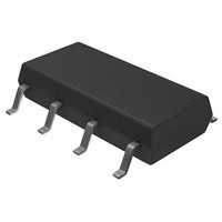
S-35399A03-J8T2G Seiko Instruments, S-35399A03-J8T2G Datasheet - Page 15

S-35399A03-J8T2G
Manufacturer Part Number
S-35399A03-J8T2G
Description
Real Time Clock 2-wire Real Time Clock
Manufacturer
Seiko Instruments
Datasheet
1.S-35399A03-J8T2G.pdf
(53 pages)
Specifications of S-35399A03-J8T2G
Supply Voltage (max)
3 V
Supply Voltage (min)
1.3 V
Maximum Operating Temperature
+ 85 C
Minimum Operating Temperature
- 40 C
Mounting Style
SMD/SMT
Rtc Bus Interface
Serial
Supply Current
0.34 uA
Package / Case
SOP-8
Lead Free Status / RoHS Status
Lead free / RoHS Compliant
Rev.2.0
INT2 pin output
(2) Output of user-set frequency
The INT1 and INT2 registers are 1-byte data registers to set up the output frequency. Setting each bit B7 to B3 in the
register to “1”, the frequency which corresponds to the bit is output in the AND-form. SC2 to SC4 in the INT1 register,
and SC5 to SC7 in the INT2 register are 3-bit SRAM type registers that can be freely set by users.
INT1 pin or
_00
Example: B7 to B3 = 50h
16 Hz
R/W
R/W
1 Hz
1 Hz
8 Hz
4 Hz
2 Hz
1 Hz
B7
B7
Figure 15 Example of output from INT1 register (Data register for output frequency)
2 Hz
R/W
2 Hz
R/W
B6
B6
Status register 2
•
Figure 13 INT1 Register (Data register for output frequency)
Figure 14 INT2 Register (Data register for output frequency)
Set to INT1FE or INT2FE = 1
R/W
R/W
4 Hz
4 Hz
B5
B5
R/W
R/W
Seiko Instruments Inc.
8 Hz
8 Hz
B4
B4
16 Hz
16 Hz
R/W
R/W
B3
B3
R/W: Read/Write
SC2
SC5
R/W
R/W
B2
B2
R/W: Read/Write
2-WIRE REAL-TIME CLOCK
SC3
SC6
R/W
R/W
B1
B1
R/W
R/W
SC4
SC7
B0
B0
S-35399A03
15


