IRF7309PBF International Rectifier, IRF7309PBF Datasheet - Page 2
IRF7309PBF
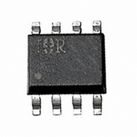
Manufacturer Part Number
IRF7309PBF
Description
MOSFET N+P 30V 3A 8-SOIC
Manufacturer
International Rectifier
Series
HEXFET®r
Type
Power MOSFETr
Specifications of IRF7309PBF
Fet Type
N and P-Channel
Fet Feature
Standard
Rds On (max) @ Id, Vgs
50 mOhm @ 2.4A, 10V
Drain To Source Voltage (vdss)
30V
Current - Continuous Drain (id) @ 25° C
4A, 3A
Vgs(th) (max) @ Id
1V @ 250µA
Gate Charge (qg) @ Vgs
25nC @ 4.5V
Input Capacitance (ciss) @ Vds
520pF @ 15V
Power - Max
1.4W
Mounting Type
Surface Mount
Package / Case
8-SOIC (3.9mm Width)
Number Of Elements
2
Polarity
N/P
Channel Mode
Enhancement
Drain-source On-volt
30V
Gate-source Voltage (max)
±20V
Power Dissipation
1.4W
Operating Temp Range
-55C to 150C
Operating Temperature Classification
Military
Mounting
Surface Mount
Pin Count
8
Package Type
SOIC
Lead Free Status / RoHS Status
Lead free / RoHS Compliant


IRF7309
Electrical Characteristics @ T
Source-Drain Ratings and Characteristics
I
L
L
V
R
V
g
I
Q
Q
Q
t
t
t
t
C
C
C
I
I
V
t
Q
t
GSS
DSS
d(on)
d(off)
f
r
SM
S
rr
on
D
S
V
fs
(BR)DSS
GS(th)
DS(ON)
iss
oss
rss
SD
g
gs
gd
rr
(BR)DSS
Repetitive rating; pulse width limited by max. junction temperature. ( See fig. 23 )
N-Channel I
P-Channel I
Pulse width
/ T
J
Gate-to-Source Forward Leakage
Drain-to-Source Breakdown Voltage
Breakdown Voltage Temp. Coefficient
Static Drain-to-Source On-Resistance
Gate Threshold Voltage
Forward Transconductance
Drain-to-Source Leakage Current
Total Gate Charge
Gate-to-Source Charge
Gate-to-Drain ("Miller") Charge
Turn-On Delay Time
Rise Time
Turn-Off Delay Time
Fall Time
Input Capacitance
Output Capacitance
Reverse Transfer Capacitance
Internal Drain Inductace
Internal Source Inductance
Continuous Source Current (Body Diode)
Pulsed Source Current (Body Diode)
Diode Forward Voltage
Reverse Recovery Time
Reverse Recovery Charge
Forward Turn-On Time
SD
SD
300µs; duty cycle
-1.8A, di/dt
2.4A, di/dt
Parameter
Parameter
73A/µs, V
90A/µs, V
2%.
DD
DD
J
= 25°C (unless otherwise specified)
V
V
(BR)DSS
(BR)DSS
, T
N-Ch 30
P-Ch -30
N-Ch — 0.032 —
P-Ch — -0.037 —
N-Ch 1.0
P-Ch -1.0
N-Ch 5.2
P-Ch 2.5
N-Ch —
P-Ch —
N-Ch —
P-Ch —
N-Ch —
P-Ch —
N-Ch —
P-Ch —
N-Ch —
P-Ch —
N-Ch —
P-Ch —
N-Ch —
P-Ch —
N-Ch —
P-Ch —
N-Ch —
P-Ch —
N-Ch —
P-Ch —
N-Ch —
P-Ch —
N-Ch —
P-Ch —
N-Ch
P-Ch
N-Ch —
N-Ch —
N-Ch —
N-Ch —
N-Ch —
, T
N-P
N-P
N-P
P-Ch —
P-Ch —
P-Ch —
P-Ch —
P-Ch —
N-P
J
148
J
Min. Typ. Max. Units
150°C
Min. Typ. Max. Units
Intrinsic turn-on time is neglegible (turn-on is dominated by L
––
—
—
—
—
—
—
150°C
520
440
180
200
6.8
7.7
4.0
6.0
11
21
17
22
25
18
72
93
—
—
— 0.050
— 0.080
—
—
—
—
—
—
—
—
—
—
— ±100
—
—
—
—
—
—
47
53
56
66
—
—
—
—
—
—
0.10
0.16
-1.0
1.0
-25
2.9
2.9
7.9
9.0
-1.8
-1.0
25
25
25
—
—
—
—
—
—
—
—
—
—
—
—
—
—
—
—
—
—
—
—
—
—
1.8
-12
1.0
16
71
80
84
99
V/°C
nC
nH
µA
ns
pF
nC
ns
V
V
S
A
V
V
V
Reference to 25°C, I
Reference to 25°C, I
V
V
V
V
V
V
V
V
V
V
V
V
V
Between lead tip
and center of die contact
N-Channel
I
P-Channel
I
N-Channel
V
R
P-Channel
V
R
N-Channel
V
P-Channel
V
T
T
N-Channel
T
P-Channel
T
D
D
GS
GS
GS
GS
GS
GS
DS
DS
DS
DS
DS
DS
DS
DS
GS
DD
DD
GS
GS
D
D
J
J
J
J
= 2.6A, V
= -2.2A, V
= 25°C, I
= 25°C, I
= 25°C, I
= 25°C, I
= 3.8
= 4.5
= V
= V
= 15V, I
= -24V, I
= 24V, V
= -24V, V
= 24V, V
= -24V, V
= 0V, I
= 0V, I
= 10V, I
= 4.5V, I
= -10V, I
= -4.5V, I
= ± 20V
= 10V, I
= -10V, I
= 0V, V
= 0V, V
GS
GS
, I
, I
D
D
DS
DS
DS
D
D
D
F
F
D
D
DS
= 250µA
D
S
S
= -250µA
D
D
GS
GS
D
D
GS
= 2.6A, di/dt = 100A/µs
= -2.2A, di/dt = 100A/µs
GS
= 250µA
= -250µA
= 2.4A
= 2.4A
= 2.6A, R
Conditions
= 1.8A, V
= -1.8A, V
= 2.0A
= -1.8A
= -1.8A
= 16V, V
= -2.2A, R
= 15V, ƒ = 1.0MHz
= -15V, ƒ = 1.0MHz
= -1.5A
= -16V, V
= 0V, T
= 0V
= 0V, T
= 0V
D
D
Conditions
= 1mA
= -1mA
J
GS
G
GS
J
GS
= 125°C
GS
G
= 125°C
= 6.0
= 4.5V
= 0V
= 6.0 ,
= 0V
= -4.5V
S
+L
D
)
Related parts for IRF7309PBF
Image
Part Number
Description
Manufacturer
Datasheet
Request
R

Part Number:
Description:
Manufacturer:
International Rectifier Corp.
Datasheet:
Part Number:
Description:
SCHOTTKY RECTIFIER
Manufacturer:
International Rectifier Corp.
Datasheet:
Part Number:
Description:
SCHOTTKY RECTIFIER
Manufacturer:
International Rectifier Corp.
Datasheet:
Part Number:
Description:
SCHOTTKY RECTIFIER
Manufacturer:
International Rectifier Corp.
Datasheet:
Part Number:
Description:
SCHOTTKY RECTIFIER
Manufacturer:
International Rectifier Corp.
Datasheet:
Part Number:
Description:
SCHOTTKY RECTIFIER
Manufacturer:
International Rectifier Corp.
Datasheet:
Part Number:
Description:
SCHOTTKY RECTIFIER
Manufacturer:
International Rectifier Corp.
Datasheet:
Part Number:
Description:
SCHOTTKY RECTIFIER
Manufacturer:
International Rectifier Corp.
Datasheet:
Part Number:
Description:
SCHOTTKY RECTIFIER
Manufacturer:
International Rectifier Corp.
Datasheet:
Part Number:
Description:
SCHOTTKY RECTIFIER
Manufacturer:
International Rectifier Corp.
Datasheet:
Part Number:
Description:
SCHOTTKY RECTIFIER
Manufacturer:
International Rectifier Corp.
Datasheet:
Part Number:
Description:
SCHOTTKY RECTIFIER
Manufacturer:
International Rectifier Corp.
Datasheet:
Part Number:
Description:
SCHOTTKY RECTIFIER
Manufacturer:
International Rectifier Corp.
Datasheet:
Part Number:
Description:
SCHOTTKY RECTIFIER
Manufacturer:
International Rectifier Corp.
Datasheet:
Part Number:
Description:
SCHOTTKY RECTIFIER
Manufacturer:
International Rectifier Corp.
Datasheet: