STGW30N120KD STMicroelectronics, STGW30N120KD Datasheet
STGW30N120KD
Specifications of STGW30N120KD
Available stocks


Related parts for STGW30N120KD


STGW30N120KD Summary of contents
Page 1
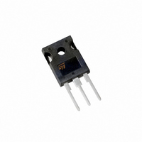
... This IGBT utilizes the advanced PowerMESH™ process resulting in an excellent trade-off between switching performance and low on-state behavior. Table 1. Device summary Order code STGW30N120KD December 2008 1200 V - short circuit rugged IGBT Figure 1. Marking Package GW30N120KD TO-247 Rev 3 STGW30N120KD TO-247 Internal schematic diagram Packaging Tube www.st.com 1/13 13 ...
Page 2
... Contents Contents 1 Electrical ratings . . . . . . . . . . . . . . . . . . . . . . . . . . . . . . . . . . . . . . . . . . . . 3 2 Electrical characteristics . . . . . . . . . . . . . . . . . . . . . . . . . . . . . . . . . . . . . 4 2.1 Electrical characteristics (curves Test circuit . . . . . . . . . . . . . . . . . . . . . . . . . . . . . . . . . . . . . . . . . . . . . . . . 9 4 Package mechanical data . . . . . . . . . . . . . . . . . . . . . . . . . . . . . . . . . . . . 10 5 Revision history . . . . . . . . . . . . . . . . . . . . . . . . . . . . . . . . . . . . . . . . . . . 12 2/13 STGW30N120KD ...
Page 3
... STGW30N120KD 1 Electrical ratings Table 2. Absolute maximum ratings Symbol V Collector-emitter voltage (V CES (1) I Collector current (continuous °C C (1) I Collector current (continuous) at 100 °C C (2) I Turn-off latching current CL (3) I Pulsed collector current CP V Gate-emitter voltage GE Short circuit withstand time SCW T = 125 ° Total dissipation at T ...
Page 4
... Gate-collector charge gc 4/13 Parameter Test conditions =125 ° =1200 =1200 V, Tc=125 ° =± Parameter Test conditions MHz 960 A STGW30N120KD Min. Typ. 1200 = 2.7 = 1mA 4 Min. Typ. Max. 2520 =0 170 GE 33 105 21 = Max. Unit V 3. 6.5 V 500 µ ± 100 nA S Unit ...
Page 5
... STGW30N120KD Table 6. Switching on/off (inductive load) Symbol t Turn-on delay time d(on) t Current rise time r (di/dt) Turn-on current slope on t Turn-on delay time d(on) t Current rise time r (di/dt) Turn-on current slope Off voltage rise time r off Turn-off delay time d off t Current fall time ...
Page 6
... Output characteristics I (A) C 120 Figure 4. Transconductance Figure 6. Gate charge vs. gate-source voltage V GE (V) V =960V CE I =20A 6/13 Figure 3. HV41160 I ( =15V GE 120 14V 90 13V 60 12V 11V 30 10V ( Figure 5. Figure 7. HV41190 80 100 Qg(nC) STGW30N120KD Transfer characteristics HV41165 V = 25V Collector-emitter on voltage vs. temperature Capacitance variations V (V) GE ...
Page 7
... STGW30N120KD Figure 8. Normalized gate threshold voltage vs. temperature Figure 10. Normalized breakdown voltage vs. temperature Figure 12. Switching losses vs. gate resistance Electrical characteristics Figure 9. Collector-emitter on voltage vs. collector current Figure 11. Switching losses vs. temperature Figure 13. Switching losses vs. collector current E (µ 780V 15V GE 4000 R = 10Ω 125˚C ...
Page 8
... Electrical characteristics Figure 14. Thermal impedance Figure 16. Forward voltage drop vs. forward current I (A) FM 100 90 T =150°C j (typical values =150° (maximum values 0.0 0.5 1.0 1.5 2.0 2.5 8/13 Figure 15. Turn-off SOA T =25°C j (maximum values) (V) 3.0 3.5 4.0 4.5 STGW30N120KD ...
Page 9
... STGW30N120KD 3 Test circuit Figure 17. Test circuit for inductive load switching Figure 19. Switching waveform Figure 18. Gate charge test circuit Figure 20. Diode recovery time waveform Test circuit 9/13 ...
Page 10
... Package mechanical data 4 Package mechanical data In order to meet environmental requirements, ST offers these devices in different grades of ECOPACK® packages, depending on their level of environmental compliance. ECOPACK® specifications, grade definitions and product status are available at: www.st.com. ECOPACK® trademark. 10/13 STGW30N120KD ...
Page 11
... STGW30N120KD Dim øP øR S TO-247 Mechanical data mm. Min. Typ 4.85 2.20 1.0 2.0 3.0 0.40 19.85 15.45 5.45 14.20 3.70 18.50 3.55 4.50 5.50 Package mechanical data Max. 5.15 2.60 1.40 2.40 3.40 0.80 20.15 15.75 14.80 4.30 3.65 5.50 11/13 ...
Page 12
... Revision history 5 Revision history Table 9. Document revision history Date 29-Jan-2008 18-Jun-2008 02-Dec-2008 12/13 Revision 1 Initial release Table 2 2 Update values in 3 Update P and R TOT thj-case STGW30N120KD Changes Table 2 Table 3) value (see and ...
Page 13
... STGW30N120KD Information in this document is provided solely in connection with ST products. STMicroelectronics NV and its subsidiaries (“ST”) reserve the right to make changes, corrections, modifications or improvements, to this document, and the products and services described herein at any time, without notice. All ST products are sold pursuant to ST’s terms and conditions of sale. ...