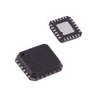
AD8341ACPZ-WP Analog Devices Inc, AD8341ACPZ-WP Datasheet

AD8341ACPZ-WP
Specifications of AD8341ACPZ-WP
Related parts for AD8341ACPZ-WP
AD8341ACPZ-WP Summary of contents
Page 1
FEATURES Cartesian amplitude and phase modulation 1.5 GHz to 2.4 GHz frequency range Continuous magnitude control of −4 −34.5 dB Continuous phase control of 0° to 360° Output third-order intercept 17.5 dBm Output 1 dB compression point 8.5 ...
Page 2
AD8341 TABLE OF CONTENTS Specifications..................................................................................... 3 Absolute Maximum Ratings............................................................ 4 ESD Caution.................................................................................. 4 Pin Configuration and Function Descriptions............................. 5 Typical Performance Characteristics ............................................. 6 Theory of Operation ...................................................................... 10 RF Quadrature Generator ......................................................... 10 I-Q Attenuators and Baseband Amplifiers.............................. 11 ...
Page 3
SPECIFICATIONS 25° Ω 1.9 GHz, single-ended, ac-coupled source drive to RFIP through 1.2 nH series inductor, RFIM ac-coupled through 1.2 nH series inductor to common, differential-to-single-ended ...
Page 4
AD8341 ABSOLUTE MAXIMUM RATINGS Table 2. Parameters Supply Voltage VPRF, VPS2 DSOP IBBP, IBBM, QBBP, QBBM RFOP, RFOM RF Input Power at Maximum Gain (RFIP or RFIM, Single-Ended Drive) Equivalent Voltage Internal Power Dissipation θ (With Pad Soldered to Board) ...
Page 5
PIN CONFIGURATION AND FUNCTION DESCRIPTIONS Table 3. Pin Function Descriptions Pin No. Mnemonic 1, 2 QFLP, QFLM 3, 4 QBBP, QBBM 5, 6, 14, 19, 24 VPS2, VPRF 7, 8, 11, 12, 20, 23 CMOP, CMRF 9, 10 RFOP, RFOM ...
Page 6
AD8341 TYPICAL PERFORMANCE CHARACTERISTICS 0 PHASE SETPOINT = 0° –5 PHASE SETPOINT = 270° –10 –15 PHASE SETPOINT = 180° –20 PHASE SETPOINT = 90° –25 –30 –35 –40 0.1 0 0.2 0.3 0.4 0.5 0.6 GAIN SETPOINT Figure 3. ...
Page 7
RF PIN = +5dBm –149 RF PIN = 0dBm –150 –151 –152 NO RF INPUT –153 –154 0 0.1 0.2 0.3 0.4 0.5 0.6 GAIN SETPOINT Figure 9. Output Noise Floor vs. Gain Setpoint, Noise in dBm/Hz, No ...
Page 8
AD8341 25 –40° +85° 1500 1600 1700 1800 1900 2000 FREQUENCY (MHz) Figure 15. Output IP3 vs. Frequency and Temperature, Maximum Gain, Phase Setpoint = 0°, 2.5 MHz Carrier Spacing –10 1V p-p BB INPUT ...
Page 9
SDD22 PORT DIFFERENTIAL S22 WITH TRANSFORMER Figure 21. Output Impedance Smith Chart 0 –10 –20 PHASE SETPOINT = 0° –30 –40 PHASE SETPOINT = 45° –50 ...
Page 10
AD8341 THEORY OF OPERATION The AD8341 is a linear RF vector modulator with Cartesian baseband controls. In the simplified block diagram given in Figure 26, the RF signal propagates from the left to the right while baseband controls are placed ...
Page 11
I-Q ATTENUATORS AND BASEBAND AMPLIFIERS The proprietary linear-responding attenuator structure is an active solution with differential inputs and outputs that offer excellent linearity, low noise, and greater immunity from mis- matches than other variable attenuator methods. The gain, in linear ...
Page 12
AD8341 APPLICATIONS USING THE AD8341 The AD8341 is designed to operate Ω impedance system. Figure 30 illustrates an example where the RF input is driven in a single-ended fashion while the differential RF out- put is converted ...
Page 13
RF OUTPUT AND MATCHING The RF outputs of the AD8341, RFOP, and RFOM, are open collectors of a transimpedance amplifier which need to be pulled up to the positive supply, preferably with RF chokes as shown in Figure 31. The ...
Page 14
AD8341 The 3 dB bandwidth is set by choosing C following equation: × 45 kHz 10 nF ≈ 3dB C 0.5 pF FLT This equation has been verified for values of C 0.1 µF (bandwidth settings of approximately ...
Page 15
REF LVL MARKER 1 [T1 ] RBW 30kHz –18.47dBm VBW 100kHz –12dBm 1.95999900GHz SWT 500ms –12 1 0.3dB OFFSET 1 [T1] –20 CH PWR ACP UP ACP LOW –30 –40 1AVG –50 –60 –70 – –90 C11 C11 ...
Page 16
AD8341 As the output power drops, the noise floor, measured in dBm in 1 MHz MHz carrier offset, drops slightly. –30 –35 ACPR 5MHz OFFSET –40 –45 ACPR 10MHz OFFSET –50 –55 –60 –65 –70 –75 NOISE ...
Page 17
EVALUATION BOARD The evaluation board circuit schematic for the AD8341 is shown in Figure 41. The evaluation board is configured to be driven from a single-ended 50 Ω source. Although the input of the AD8341 is differential, it may be ...
Page 18
AD8341 Components Function C2, C4, C7, Supply Decoupling. C9, C14, C1, C3, C8, C10, R2, R4, R5, R6 R8, SW1 Output Disable Interface. The output stage of the AD8341 is disabled by applying a high voltage to the DSOP pin ...
Page 19
Figure 42. Component Side Layout Figure 43. Component Side Silkscreen Rev Page AD8341 ...
Page 20
... PIN 1 INDICATOR 1.00 0.85 0.80 SEATING PLANE ORDERING GUIDE Model Temperature Range 1, 2 AD8341ACPZ-WP −40°C to +85°C AD8341ACPZ-REEL7 2 −40°C to +85°C AD8341-EVAL Waffle pack Pb-free part. © 2004 Analog Devices, Inc. All rights reserved. Trademarks and regis- tered trademarks are the property of their respective owners. ...


