ADAU1445YSVZ-3A-RL Analog Devices Inc, ADAU1445YSVZ-3A-RL Datasheet - Page 87
ADAU1445YSVZ-3A-RL
Manufacturer Part Number
ADAU1445YSVZ-3A-RL
Description
175MHZ SigmaDSP,2x8 SRCs
Manufacturer
Analog Devices Inc
Series
SigmaDSP®r
Type
Audio Processorr
Specifications of ADAU1445YSVZ-3A-RL
Applications
Automotive Audio
Mounting Type
Surface Mount
Package / Case
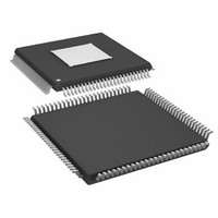
100-TQFP Exposed Pad, 100-eTQFP, 100-HTQFP, 100-VQFP
Format
Fixed Point
Program Memory Size
Not RequiredKB
Operating Supply Voltage (typ)
1.8/3.3V
Operating Temp Range
-40C to 105C
Operating Temperature Classification
Industrial
Mounting
Surface Mount
Pin Count
100
Lead Free Status / RoHS Status
Lead free / RoHS Compliant
Lead Free Status / RoHS Status
Lead free / RoHS Compliant
Available stocks
Company
Part Number
Manufacturer
Quantity
Price
Company:

Part Number:
ADAU1445YSVZ-3A-RL
Manufacturer:
Analog Devices Inc
Quantity:
10 000


APPLICATIONS INFORMATION
LAYOUT RECOMMENDATIONS
Parts P
All 100
a
cl
The AVDD, DVDD, PVDD, and IO
board sh
capacitor (
All trac
kept as
should
oscillato
crystal
Groun
A single
Compo
from dig
Expose
The AD
for imp
a packag
•
•
nalog, digital, and PLL power-ground pair, should be placed as
ose to the ADAU1442/ADAU1445/ADAU1446 as possible.
A co
on
co
Fi
Vi
fo
see
the
gure 60).
r efficien
as should be laced to co
nnect so
startup
ding
es in th
short a
not be a
roved h
nents in
nF bypass
AU144
lacemen
all laye
d Pad
r circu
e, spec
Figure
pad ar
ould each b
groun
ital sig
pper l
10 μ
Figur
s possi
F to 4
2 and A
ial cons
e crystal oscillator circuit (Figure 9) should be
it com
d plan
rs of t
ea.
e 60. Ex
and op
PCB D
eat diss
ny lon
nals.
ayer e
mew
61, w
t hea
an an
t
capaci
p
e bypassed ith an additional single bulk
7 μF).
here to a de
t and energ
he board,
hich has 16
ble to mi
VIAS
e should
qual in si
posed Pad
ponents
g board
alog sign
ideration
eration.
esign
DAU144
ipation.
tors, w
nimize stray capacitance. There
traces connected to crystal
because such traces may affect
be used in the application layou
ze to the exposed pad should be
Layout Example—Side View
5 packages include an exposed pa
al path should be placed away
When designing a board for su
from top to bottom
nnect all layers of cop
should be given to the following:
w
hich are recommended for every
y conductivity. F
COPPER SQUARES
dicated copper b
vias arranged in
VDD supply signals on the
TOP
GROUND
POWER
BOTTOM
or
oard layer (see
a 4 × 4 grid in
, and should
per
an example,
, allowing
Rev. C | Page 87 of 92
ch
t.
d
PLL Loop Filter
The single resistor an
should be connected
short traces to minim
Power Supply Bypa
Each power supply p
appropriate ground p
connections to each
possible, and the trac
For maximum effect
located either equidi
when equidistant pla
power pin. Thermal
on the far side of the
EOS/ESD Protectio
Although the ADAU
internal protection cir
discharge, an externa
recommended for al
Examples can be foun
Analog Devices webs
Figure 62. Recomm
Figure 61. Ex
ADAU1442/ADAU1445/ADAU1446
TO POWER
CAPACITOR
l systems to preve
side of the capacit
iveness, the capaci
stant from the powe
connections to th
in should be bypa
1442/ADAU1445
d in the AN-311 A
cement is not pos
n
cuitry against over
posed Pad Layout Ex
e should stay on a si
capacitor.
ended Power Supply
l transient voltag
to the PLL_FILT
ite.
d two capacitors
in with a single 1
ize jitter.
ss Capacitors
POWER GROUND
TO GR
e suppressor (TVS) is
e planes should be made
nt damage to the IC.
in the PLL loop filter
/ADAU1446 have robust
00 nF capacitor. The
or should be as short as
ample—Top View
and PVDD pins with
ssed to its nearest
sible, slightly closer to the
Bypass Capacitor Layout
voltages and electrostatic
pplication Note on the
tor should preferably be
OUND
r and ground pins or,
ngle layer with no vias.
Related parts for ADAU1445YSVZ-3A-RL
Image
Part Number
Description
Manufacturer
Datasheet
Request
R

Part Number:
Description:
SigmaDSP� Digital Audio Processor with Flexible Audio Routing Matrix
Manufacturer:
Analog Devices
Datasheet:

Part Number:
Description:
±1.7g Dual-Axis IMEMS Accelerometer Evaluation Board
Manufacturer:
Analog Devices Inc
Datasheet:

Part Number:
Description:
Inertial Sensor Evaluation System
Manufacturer:
Analog Devices Inc
Datasheet:
Part Number:
Description:
Manufacturer:
Analog Devices Inc
Datasheet:
Part Number:
Description:
Manufacturer:
Analog Devices Inc
Datasheet:
Part Number:
Description:
Manufacturer:
Analog Devices Inc
Datasheet:
Part Number:
Description:
Manufacturer:
Analog Devices Inc
Datasheet:
Part Number:
Description:
Manufacturer:
Analog Devices Inc
Datasheet:
Part Number:
Description:
Manufacturer:
Analog Devices Inc
Datasheet:
Part Number:
Description:
Manufacturer:
Analog Devices Inc
Datasheet:
Part Number:
Description:
Manufacturer:
Analog Devices Inc
Datasheet:
Part Number:
Description:
Manufacturer:
Analog Devices Inc
Datasheet:
Part Number:
Description:
Manufacturer:
Analog Devices Inc
Datasheet: