ADA4857-1YCPZ-R7 Analog Devices Inc, ADA4857-1YCPZ-R7 Datasheet
ADA4857-1YCPZ-R7
Specifications of ADA4857-1YCPZ-R7
Available stocks


Related parts for ADA4857-1YCPZ-R7


ADA4857-1YCPZ-R7 Summary of contents
Page 1
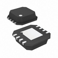
... With a wide supply voltage range ( V), the ADA4857 is an ideal candidate for systems that require high dynamic range, precision, and speed. The ADA4857-1 amplifier is available × 3 mm, 8-lead LFCSP and a standard 8-lead SOIC. The ADA4857-2 is available × 4 mm, 16-lead LFCSP. The LFCSP features an exposed paddle that provides a low thermal resistance path to the printed circuit board (PCB) ...
Page 2
... ADA4857-1/ADA4857-2 TABLE OF CONTENTS Features .............................................................................................. 1 Applications ....................................................................................... 1 Connection Diagrams ...................................................................... 1 General Description ......................................................................... 1 Revision History ............................................................................... 2 Specifications ..................................................................................... 3 ±5 V Supply ................................................................................... Supply ................................................................................... 4 Absolute Maximum Ratings ............................................................ 6 Thermal Resistance ...................................................................... 6 Maximum Power Dissipation ..................................................... 6 ESD Caution .................................................................................. 6 Pin Configurations and Function Descriptions ........................... 7 Typical Performance Characteristics ............................................. 9 REVISION HISTORY 11/08—Rev Rev. A Changes to Table 5 ............................................................................ 7 Changes to Table 7 ............................................................................ 8 Changes to Figure 32 ...................................................................... 13 Added Figure 44 ...
Page 3
... Chip enabled Chip powered down Common mode Differential mode Common mode V = ± ±2 kΩ 100 Ω L Sinking and sourcing 30% overshoot Rev Page ADA4857-1/ADA4857-2 Min Typ 650 850/750 600/550 400/350 110 75/90 2800 15 −108 −108 −88 −93 −65 −62 4.4 1.5 ±2 2.3 − ...
Page 4
... ADA4857-1/ADA4857-2 Parameter POWER SUPPLY Operating Range Quiescent Current Quiescent Current (Power Down) Positive Power Supply Rejection Negative Power Supply Rejection +5 V SUPPLY T = 25° + 499 Ω Table 2. Parameter DYNAMIC PERFORMANCE –3 dB Bandwidth (LFCSP/SOIC) Full Power Bandwidth Bandwidth for 0.1 dB Flatness (LFCSP/SOIC) Slew Rate (10% to 90%) Settling Time to 0 ...
Page 5
... Quiescent Current (Power Down) Positive Power Supply Rejection Negative Power Supply Rejection Conditions kΩ 100 Ω L Sinking and sourcing 30% overshoot ≥ V − 4 5.5 V, − −V = −0 +0 Rev Page ADA4857-1/ADA4857-2 Min Typ Max Unit 1 4.5 10 250 350 μA −58 − ...
Page 6
... The power dissipated in the package (P quiescent power dissipation and the power dissipated in the Rating die due to the ADA4857 drive at the output. The quiescent 11 V power is the voltage between the supply pins (V See Figure 4 quiescent current (I − ...
Page 7
... GND or V Exposed Pad. The exposed pad S may be connected to GND Table 6. 8-Lead SOIC Pin Function Descriptions Pin No Rev Page ADA4857-1/ADA4857 ADA4857-1 – TOP VIEW +IN OUT 3 6 (Not to Scale) – CONNECT Figure 6. 8-Lead SOIC Pin Configuration Mnemonic Description FB Feedback −IN Inverting Input ...
Page 8
... FB2 9 −IN2 10 +IN2 12 − OUT1 PD1 16 FB1 EP GND or Vs –IN1 1 12 –V S1 ADA4857-2 +IN1 TOP VIEW +IN2 (Not to Scale) – –IN2 CONNECT Figure 7. 16-Lead LFCSP Pin Configuration Description Inverting Input 1. Noninverting Input 1. No Connect. Negative Supply 2. Output 2. Positive Supply 2. Power Down 2. ...
Page 9
... Figure 12. Small Signal Frequency Response for Various Capacitive Loads (LFCSP –40°C –1 –2 –3 –4 –5 –6 +25°C –7 +125°C –8 –9 –10 1000 1 Figure 13. Large Signal Frequency Response vs. V Rev Page ADA4857-1/ADA4857 + ± 1kΩ p-p OUT 10 100 1000 FREQUENCY (MHz) 10pF 5pF NO CAP LOAD ± ...
Page 10
... ADA4857-1/ADA4857 100Ω –1 –2 –3 – – ±5V S – 0.2V p-p OUT – 100 FREQUENCY (MHz) Figure 14. Small Signal Frequency Response for Various Resistive Loads (LFCSP –1 –2 –3 – +10 –5 – –7 – 1kΩ – 0.2V p-p OUT –10 ...
Page 11
... Figure 24. 0.1 dB Flatness vs. Frequency for Various Output Voltages (LFCSP) 2 ± 1kΩ 2 1.5 1.0 0.5 0 –0.5 –1.0 –1.5 –2.0 –2.5 Figure 25. Large Signal Transient Response for Various Output Voltages (LFCSP) Rev Page ADA4857-1/ADA4857-2 V OUT OUTPUT INPUT TIME (5ns/DIV) Figure 23. Short-Term Settling Time (LFCSP ± 150Ω OUT V = 0.2V p-p ...
Page 12
... ADA4857-1/ADA4857-2 0.25 0.20 0.15 0. 1.5pF 0. –0.05 –0.10 –0.15 –0.20 –0.25 TIME (10ns/DIV) Figure 26. Small Signal Transient Response for Various Capacitive Loads (LFCSP) 0.25 0.20 0. ±5V S 0.10 0. ±2. –0.05 –0.10 –0.15 –0.20 –0.25 TIME (10ns/DIV) Figure 27. Small Signal Transient Response for Various Supply Voltages (LFCSP) ...
Page 13
... Figure 36. Output Overdrive Recovery for Various Resistive Loads –30 –40 –50 –60 –70 –80 –90 100 1000 0.1 Figure 37. Common-Mode Rejection Ratio (CMRR) vs. Frequency Rev Page ADA4857-1/ADA4857 ± 1kΩ LFCSP 1 10 100 FREQUENCY (MHz) Figure 35. PD Isolation vs. Frequency V = ± ...
Page 14
... ADA4857-1/ADA4857-2 100 V = ± 100 1k 10k FREQUENCY (Hz) Figure 38. Input Current Noise vs. Frequency 238 MEAN: 5.00 SD: 0. 4.85 4.90 4.95 5.00 SUPPLY CURRENT (mA) Figure 39. Supply Current 100k 1M 5.05 5.10 5.15 Rev Page 1000 100 100 1k 10k FREQUENCY (Hz) Figure 40. Input Voltage Noise vs. Frequency 3.5 3 ...
Page 15
... S Figure 44. Typical Capacitive Load Configuration (LFCSP) 0.1µF V OUT OUT R L 0.1µF V OUT Rev Page ADA4857-1/ADA4857 10µF 1kΩ 0.1µF 1kΩ V 1kΩ IN 53.6Ω 1kΩ 10µF 0.1µF –V S Figure 45. Common-Mode Rejection +V S 10µF 0.1µF V ...
Page 16
... PD pin input voltage is low (see Table 8). Note that PD does not put the output in a high-Z state, which means that the ADA4857 should not be used as a multiplexer. Table 8. PD Operation Table Guide ...
Page 17
... IF strips. With a 410 MHz gain bandwidth product and high slew rate, the ADA4857 ideal candidate for active filters. Figure 48 shows the frequency response of 90 MHz and 45 MHz LPFs. In addition to the bandwidth requirements, the slew rate must be capable of supporting the full power bandwidth of the filter ...
Page 18
... The returns for the input, output terminations, bypass capacitors, and R close to the ADA4857 as possible. The output load ground and the bypass capacitor grounds should be returned to the same point on the ground plane to minimize parasitic trace inductance, ringing, and overshoot and to improve distortion performance ...
Page 19
... CONTROLLING DIMENSIONS ARE IN MILLIMETERS; INCH DIMENSIONS (IN PARENTHESES) ARE ROUNDED-OFF MILLIMETER EQUIVALENTS FOR REFERENCE ONLY AND ARE NOT APPROPRIATE FOR USE IN DESIGN. Figure 52. 8-Lead Standard Small Outline Package [SOIC_N] (R-8) Dimensions shown in millimeters and (inches) Rev Page ADA4857-1/ADA4857-2 0.50 BSC 5 8 1.60 EXPOSED 1 ...
Page 20
... ORDERING GUIDE Model Temperature Range ADA4857-1YCPZ-R2 1 –40°C to +125°C 1 ADA4857-1YCPZ-RL –40°C to +125°C 1 ADA4857-1YCPZ-R7 –40°C to +125°C 1 ADA4857-1YRZ –40°C to +125°C 1 ADA4857-1YRZ-R7 –40°C to +125°C 1 ADA4857-1YRZ-RL –40°C to +125°C 1 ADA4857-2YCPZ-R2 –40°C to +125°C ...