MGP15N35CL ON Semiconductor, MGP15N35CL Datasheet

IGBT Transistors 15A 350V Ignition

MGP15N35CL

Manufacturer Part Number
MGP15N35CL
Description
IGBT Transistors 15A 350V Ignition
Manufacturer
ON Semiconductor
Datasheet

Specifications of MGP15N35CL

Configuration
Single
Collector- Emitter Voltage Vceo Max
380 V
Collector-emitter Saturation Voltage
10 V
Maximum Gate Emitter Voltage
22 V
Gate-emitter Leakage Current
150 W
Power Dissipation
150 W
Maximum Operating Temperature
+ 175 C
Package / Case
TO-220-3
Continuous Collector Current Ic Max
15 A
Minimum Operating Temperature
- 55 C
Mounting Style
Through Hole
Channel Type
N
Collector Current (dc) (max)
15A
Package Type
TO-220AB
Pin Count
3 +Tab
Mounting
Through Hole
Operating Temperature (min)
-55
Operating Temperature (max)
175C
Operating Temperature Classification
Military
Transistor Type
IGBT
Dc Collector Current
15A
Collector Emitter Voltage Vces
360V
Power Dissipation Pd
150W
Collector Emitter Voltage V(br)ceo
360V
Operating Temperature Range
-55°C To +175°C
Rohs Compliant
No
Lead Free Status / RoHS Status
Lead free / RoHS Compliant

Available stocks

Company
Part Number
Manufacturer
Quantity
Price
Part Number:
MGP15N35CL
Manufacturer:
ON
Quantity:
12 500
MGP15N35CL,
MGB15N35CL
Ignition IGBT
15 Amps, 350 Volts
N−Channel TO−220 and D
monolithic circuitry integrating ESD and Over−Voltage clamped
protection for use in inductive coil drivers applications. Primary uses
include Ignition, Direct Fuel Injection, or wherever high voltage and
high current switching is required.
MAXIMUM RATINGS
UNCLAMPED COLLECTOR−TO−EMITTER AVALANCHE
CHARACTERISTICS
© Semiconductor Components Industries, LLC, 2006
July, 2006 − Rev. 5
Collector−Emitter Voltage
Collector−Gate Voltage
Gate−Emitter Voltage
Collector Current−Continuous
ESD (Human Body Model)
ESD (Machine Model) R = 0 Ω, C = 200 pF
Total Power Dissipation @ T
Operating and Storage Temperature Range
Single Pulse Collector−to−Emitter Avalanche
Reverse Avalanche Energy
This Logic Level Insulated Gate Bipolar Transistor (IGBT) features
System Applications
Stress Applied to Load
Microprocessor Devices
Ideal for Coil−On−Plug, IGBT−On−Coil, or Distributorless Ignition
High Pulsed Current Capability up to 50 A
Gate−Emitter ESD Protection
Temperature Compensated Gate−Collector Voltage Clamp Limits
Integrated ESD Diode Protection
Low Threshold Voltage to Interface Power Loads to Logic or
Low Saturation Voltage
Optional Gate Resistor (R
@ T
R = 1500 Ω, C = 100 pF
Derate above 25°C
Energy
V
= 2.0 mH, Starting T
V
= 2.0 mH, Starting T
V
Pk I
CC
CC
CC
L
C
= 50 V, V
= 50 V, V
= 100 V, V
= 25.8 A, Starting T
= 25°C − Pulsed
Characteristic
GE
GE
GE
Rating
= 5.0 V, Pk I
= 5.0 V, Pk I
= 20 V, L = 3.0 mH,
J
J
(−55°C ≤ T
(−55°C ≤ T
= 25°C
= 150°C
J
C
Preferred Device
= 25°C
G
= 25°C
L
L
)
= 17.4 A, L
= 14.2 A, L
J
J
≤ 175°C)
≤ 175°C unless otherwise noted)
2
PAK
Symbol
Symbol
E
T
E
V
V
AS(R)
ESD
ESD
J
V
P
, T
AS
CES
CER
I
GE
C
D
stg
Value
−55 to
Value
1000
300
200
380
380
800
150
175
8.0
1.0
22
15
50
1
Watts
W/°C
Unit
V
V
V
A
Unit
A
mJ
mJ
kV
°C
V
DC
DC
DC
DC
AC
Preferred devices are recommended choices for future use
and best overall value.
MGP15N35CL
MGB15N35CLT4
Gate
1
2
1
Device
V
3
G15N35CL
YWW
Collector
R
CE(on)
Collector
G
GE
350 VOLTS (Clamped)
4
ORDERING INFORMATION
2
4
CASE 221A
MARKING DIAGRAMS
TO−220AB
& PIN ASSIGNMENTS
STYLE 9
http://onsemi.com
15 AMPERES
3
Emitter
@ 10 A = 1.8 V Max
N−Channel
Package
R
TO−220
D2PAK
G15N35CL = Device Code
Y
WW
G
Publication Order Number:
Gate
C
E
1
1
G15N35CL
YWW
800 Tape & Reel
Collector
Collector
= Year
= Work Week
MGP15N35CL/D
CASE 418B
2
50 Units/Rail
STYLE 4
Shipping
3
D
2
4
2
PAK
3
Emitter
4

Related parts for MGP15N35CL

MGP15N35CL Summary of contents

Page 1

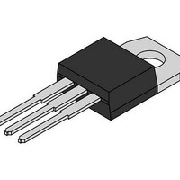
... STYLE 9 MARKING DIAGRAMS 3 & PIN ASSIGNMENTS 4 4 Collector Collector G15N35CL YWW G15N35CL YWW 1 3 Gate Emitter Collector Emitter 2 G15N35CL = Device Code Collector Y = Year WW = Work Week ORDERING INFORMATION Device Package Shipping TO−220 50 Units/Rail D2PAK 800 Tape & Reel Publication Order Number: MGP15N35CL/D 4 ...

Page 2

THERMAL CHARACTERISTICS Characteristic Thermal Resistance, Junction to Case Thermal Resistance, Junction to Ambient Maximum Lead Temperature for Soldering Purposes, 1/8″ from case for 5 seconds ELECTRICAL CHARACTERISTICS Characteristic OFF CHARACTERISTICS Collector−Emitter Clamp Voltage Zero Gate Voltage Collector Current Reverse Collector−Emitter ...

Page 3

ELECTRICAL CHARACTERISTICS Characteristic ON CHARACTERISTICS (continued) Collector−to−Emitter On−Voltage Collector−to−Emitter On−Voltage Forward Transconductance DYNAMIC CHARACTERISTICS Input Capacitance Output Capacitance Transfer Capacitance SWITCHING CHARACTERISTICS (Note 3) Turn−Off Delay Time (Inductive) Fall Time (Inductive) Turn−Off Delay Time (Resistive) Fall Time (Resistive) Turn−On Delay ...

Page 4

TYPICAL ELECTRICAL CHARACTERISTICS (unless otherwise noted 10 5 25° COLLECTOR TO EMITTER VOLTAGE (VOLTS) CE ...

Page 5

T = 25° 150° INDUCTOR (mH) Figure 7. Minimum Open Secondary Latch Current vs. Inductor 25° 150° ...

Page 6

R , EXTERNAL GATE RESISTANCE (Ω) G Figure 13. Switching Speed vs. External Gate Resistance 10 Duty Cycle = 0.5 1 0.2 0.1 0.05 0.02 ...

Page 7

Figure 16. Test Fixture for Transient Thermal Curve (48 square inches of 1/8, thick aluminum) 100 100 ms 0.1 0. COLLECTOR−EMITTER VOLTAGE (VOLTS) Figure 17. Single Pulse Safe Operating Area (Mounted on an Infinite ...

Page 8

(pk 0 DUTY CYCLE 0. COLLECTOR−EMITTER VOLTAGE ...

Page 9

PACKAGE DIMENSIONS TO−220 THREE−LEAD TO−220AB CASE 221A−09 ISSUE AA NOTES: SEATING −T− 1. DIMENSIONING AND TOLERANCING PER ANSI PLANE Y14.5M, 1982. 2. ...

Page 10

... J 0.018 0.025 0.46 0.64 K 0.090 0.110 2.29 2.79 S 0.575 0.625 14.60 15.88 V 0.045 0.055 1.14 1.40 STYLE 4: PIN 1. GATE 2. COLLECTOR 3. EMITTER 4. COLLECTOR ON Semiconductor Website: www.onsemi.com Order Literature: http://www.onsemi.com/orderlit For additional information, please contact your local Sales Representative MGP15N35CL/D ...

Related keywords