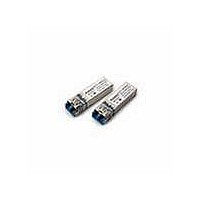
HFCT-5953TL Avago Technologies US Inc., HFCT-5953TL Datasheet - Page 9

HFCT-5953TL
Manufacturer Part Number
HFCT-5953TL
Description
Fiber Optic Transmitters, Receivers, Transceivers OC12 IR 2x5 SFF LC
Manufacturer
Avago Technologies US Inc.
Datasheet
1.HFCT-5953TL.pdf
(17 pages)
Specifications of HFCT-5953TL
Function
High performance, modules for serial optical data communication applications, designed for single mode fiber.
Product
Transceiver
Data Rate
622 Mbps
Wavelength
1300 nm
Maximum Rise Time
1 ns, 0.5 ns
Maximum Fall Time
1 ns, 0.5 ns
Maximum Output Current
50 mA
Operating Supply Voltage
3.14 V to 3.47 V
Maximum Operating Temperature
+ 70 C
Minimum Operating Temperature
0 C
Package / Case
DIP-10 with Connector
Optical Fiber Type
TX/RX
Data Transfer Rate
622Mbps
Optical Rise Time
1/0.5ns
Optical Fall Time
1/0.5ns
Operating Temperature Classification
Commercial
Peak Wavelength
1356/1570nm
Package Type
DIP With Connector
Operating Supply Voltage (min)
3.14V
Operating Supply Voltage (typ)
3.3V
Operating Supply Voltage (max)
3.47V
Output Current
50mA
Operating Temp Range
0C to 70C
Mounting
Snap Fit To Panel
Pin Count
10
For Use With
Singlemode Glass
Lead Free Status / RoHS Status
Lead free / RoHS Compliant
T
Figure 8 - Recommended Interface Circuit (HFCT-5953xxx)
The HFCT-5953xxx/HFCT-5954xxx have a transmit disable
function which is a single-ended +3.3 V TTL input which
is dc-coupled to pin 13 on the HFCT-5954xxx and pin 8
on HFCT- 5953xxx. In addition the HFCT-5954xxx offers
the designer the option of monitoring the laser diode bias
current and the laser diode optical power. The voltage
measured between pins 17 and 18 is proportional to the
bias current through an internal 10 Ω resistor. Similarly
the optical power rear facet monitor circuit provides
a photo current which is proportional to the voltage
measured between pins 19 and 20 on the 2 x 10 ver-
sion, this voltage is measured across an internal 200 Ω
resistor.
As for the receiver section, it is internally ac-coupled
between the preamplifier and the postamplifier stages.
The actual Data and Data-bar outputs of the postampli-
fier are dc-coupled to their respective output pins (pins
9 and 10 on the HFCT-5953xxx and pins 14 and 15 on
the HFCT-5954xxx). The two data outputs of the re-
ceiver should be terminated with identical load circuits
to avoid unnecessarily large ac currents in V
puts are loaded identically the ac current is largely nulled.
9
Note:
Note A: CIRCUIT ASSUMES OPEN EMITTER OUTPUT
Note B: WHEN INTERNAL BIAS IS PROVIDED REPLACE SPLIT RESISTORS WITH 100 W TERMINATION
* C4 IS AN OPTIONAL BYPASS CAPACITOR FOR ADDITIONAL LOW FREQUENCY NOISE FILTERING.
DIS
T
R
X
X
(LVTTL)
C1 = C2 = C3 = 10 nF or 100 nF
10
1
9
2
8
3
7
130 Ω
4
V
82 Ω
130 Ω
CC
6
CC
(+3.3 V)
See Figure 7a
5
. If the out-
82 Ω
130 Ω
130 Ω
C2
C1
100 nF
100 nF
100 nF
100 nF
100 nF
10 µF
C4 *
10 µF
Signal Detect is a single-ended, +3.3 V TTL compatible out-
put signal that is dc-coupled to pin 3 on the HFCT-5953xxx
and pin 8 on the HFCT-5954xxx modules. Signal Detect
should not be ac-coupled externally to the follow-on cir-
cuits because of its infrequent state changes.
The HFCT-5954xxx offers the designer the option of moni-
toring the PIN photo detector bias current. Figures 7 and 8
show a resistor network, which could be used to do this.
Note that the photo detector bias current pin must
be connected to V
mends that a decoupling capacitor is used on this pin.
1 µH
1 µH
Z = 50 Ω
Z = 50 Ω
Z = 50 Ω
Z = 50 Ω
V
CC
(+3.3 V)
C3
100 nF
BY THE HFCT-5953ATL/TL
THIS IS NOT REQUIRED
130 Ω
82 Ω
130 Ω
CC
10 k Ω
V
CC
. Avago Technologies also recom-
(+3.3 V)
V
CC
82 Ω
130 Ω
(+3.3 V)
TD-
TD+
RD+
RD-
SD
130
Ω
LVTTL
V
CC
V
(+3.3 V)
CC
(+3.3 V)
NOTE A
NOTE B


