LM5007EVAL National Semiconductor, LM5007EVAL Datasheet - Page 5
LM5007EVAL
Manufacturer Part Number
LM5007EVAL
Description
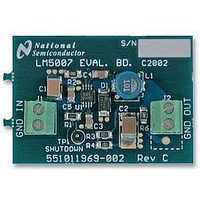
EVALUATION BOARD KIT, LM5007 SERIES
Manufacturer
National Semiconductor
Datasheet
1.LM5007EVAL.pdf
(12 pages)
Specifications of LM5007EVAL
Svhc
No SVHC (15-Dec-2010)
Development Tool Type
Evaluation Board
Kit Features
12V To 75V Input Range, 90% Measured Efficiency, 10V Output Voltage, 400mA Output Current
Silicon Manufacturer
National Semiconductor
Kit Contents
Board, Datasheet
Features
Thermal Shutdown, Intelligent Current Limit Protection, Highly Efficient Operation
Available stocks
Company
Part Number
Manufacturer
Quantity
Price
Company:

Part Number:
LM5007EVAL/NOPB
Manufacturer:
National Semiconductor
Quantity:
135


Minimum Off Time
Regulation and OV Comparators
Thermal Shutdown
Tsd
Thermal Resistance
θ
JA
Electrical Characteristics
Specifications with standard typeface are for T
Temperature range. V
Note 1: Absolute Maximum Ratings are limits beyond which damage to the device may occur. Operating Ratings are conditions under which operation of the device
is intended to be functional. For guaranteed specifications and test conditions, see the Electrical Characteristics.
Note 2: For detailed information on soldering plastic MSOP and LLP packages, refer to the Packaging Data Book available from National Semiconductor
Corporation.
Note 3: All limits are guaranteed. All electrical characteristics having room temperature limits are tested during production with T
are guaranteed by correlating the electrical characteristics to process and temperature variations and applying statistical process control.
Note 4: The V
Note 5: The human body model is a 100pF capacitor discharge through a 1.5kΩ resistor into each pin. The machine model is a 200pF capacitor discharged directly
into each pin. The machine model ESD compliance level for Pin 5 is 150V. The human body ESD compliance level for Pin 7 and 8 is 1000V.
Note 6: For devices procurred in the LLP-8 package the Rds(on) limits are guaranteed by design characterization data only.
Detailed Operating Description
The LM5007 Step Down Switching Regulator features all of
the functions needed to implement low cost, efficient, Buck
bias regulators. This high voltage regulator contains an 80V,
0.7A N-Channel Buck Switch. The device is easy to apply
and is provided in the MSOP-8 and the thermally enhanced
LLP-8 packages. The regulator is based on a hysteretic
control scheme using an on time inversely proportional to
Vin. This feature allows the operating frequency to remain
relatively constant with load and input voltage variations. The
hysteretic control requires no control loop compensation,
while providing very fast load transient response. An intelli-
gent current limit scheme is implemented in the LM5007 with
forced off time, after current limit detection, which is in-
versely proportional to Vout. This current limiting scheme
reduces load current foldback. Additional protection features
include: Thermal Shutdown, Vcc undervoltage lockout, Gate
drive undervoltage lockout and Max Duty Cycle limiter. The
LM5007 can be applied in numerous applications to effi-
ciently regulate step down higher voltage inputs. This regu-
lator is well suited for 48 Volt Telcom and the new 42V
Automotive power bus ranges.
Hysteretic Control Circuit
Overview
The LM5007 is a Buck DC-DC regulator that uses an on time
control scheme. The on time is programmed by an external
resistor and varies inversely with line input voltage (Vin). The
core regulation elements of the LM5007 are the feedback
comparator and the on time one-shot. The regulator output
voltage is sensed at the feedback pin (FB) and is compared
to an internal reference voltage (2.5V). If the FB signal is
below the reference voltage, the buck switch is turned on for
Symbol
CC
Minimum Off Timer
FB Reference Threshold
FB Over-Voltage Threshold
FB Bias Current
Thermal Shutdown Temp.
Thermal Shutdown Hysteresis
Junction to Ambient
output is intended as a self bias for the internal gate drive power and control circuits. Device thermal limitations limit external loading.
Parameter
IN
= 48V, unless otherwise stated (Note 3).
(Continued)
FB = 0V
Internal reference
Trip point for switch ON
Trip point for switch OFF
MUA Package
SDC Package
J
= 25˚C, and those with boldface type apply over full Operating Junction
Conditions
5
a fixed time pulse determined by the line voltage and a
programming resistor (R
switch will remain off for at least the minimum off timer period
of 300ns. If the FB pin voltage is still below the reference
after the 300ns off time, the switch will turn on again for
another on time period. This switching behavior will continue
until the FB pin voltage reaches the reference voltage level.
The LM5007 operates in discontinuous conduction mode at
light load currents or continuous conduction mode at heavier
load currents. In discontinuous conduction mode, current
through the output inductor starts at zero and ramps up to a
peak value during the buck switch on time and then back to
zero during the off time. The inductor current remains at zero
until the next on time period starts when FB falls below the
internal reference. In discontinuous mode the operating fre-
quency can be relatively low and will vary with load. There-
fore at light loads the conversion efficiency is maintained,
since the switching losses decrease with the reduction in
load current and switching frequency. The approximate dis-
continuous mode operating frequency can be calculated as
follows:
In continuous conduction mode, current flows continuously
through the inductor and never ramps down to zero. In this
mode the operating frequency is greater than the discontinu-
ous mode frequency and remains relatively constant with
load and line variations. The approximate continuous mode
operating frequency can be calculated as follows:
2.445
Min
2.875
Typ
300
100
165
200
2.5
25
40
ON
). Following the on period the
A
= T
J
2.550
= 25˚C. All hot and cold limits
Max
www.national.com
Units
˚C/W
˚C/W
nA
ns
˚C
˚C
V
V
Related parts for LM5007EVAL
Image
Part Number
Description
Manufacturer
Datasheet
Request
R

Part Number:
Description:
National Semiconductor [8-Bit D/A Converter]
Manufacturer:
National Semiconductor
Datasheet:
Part Number:
Description:
National Semiconductor [Media Coprocessor]
Manufacturer:
National Semiconductor
Datasheet:
Part Number:
Description:
Digitally Controlled Tone and Volume Circuit with Stereo Audio Power Amplifier, Microphone Preamp Stage and National 3D Sound
Manufacturer:
National Semiconductor
Datasheet:
Part Number:
Description:
Digitally Controlled Tone and Volume Circuit with Stereo Audio Power Amplifier, Microphone Preamp Stage and National 3D Sound
Manufacturer:
National Semiconductor
Datasheet:
Part Number:
Description:
AC97 Rev 2 Codec with Sample Rate Conversion and National 3D Sound
Manufacturer:
National Semiconductor
Part Number:
Description:
Manufacturer:
National Semiconductor
Datasheet:
Part Number:
Description:
Manufacturer:
National Semiconductor
Datasheet:
Part Number:
Description:
General Purpose, Low Voltage, Low Power, Rail-to-Rail Output Operational Amplifiers
Manufacturer:
National Semiconductor
Datasheet:
Part Number:
Description:
8-bit 20 MSPS flash A/D converter.
Manufacturer:
National Semiconductor
Datasheet:
Part Number:
Description:
Low Noise Quad Operational Amplifier
Manufacturer:
National Semiconductor
Datasheet:
Part Number:
Description:
Quad Differential Line Receivers
Manufacturer:
National Semiconductor
Datasheet:
Part Number:
Description:
Quad High Speed Trapezoidal? Bus Transceiver
Manufacturer:
National Semiconductor
Datasheet:
Part Number:
Description:
Dual Line Receiver
Manufacturer:
National Semiconductor
Datasheet:
Part Number:
Description:
TTL to 10k ECL Level Translator with Latch
Manufacturer:
National Semiconductor
Datasheet: