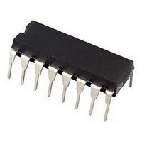
Functional Description:
The NTE2632 is a quad line receiver constructed using Advanced Low–Power Schottky processing
in a 16–Lead DIP type package designed to meet the requirements of RS–422 and RS–423, and fed-
eral standards 1020 and 1030 for balanced and unbalanced digital data transmission. This device
features and input sensitivity of 200mV over the input voltage range of 7V.
The NTE2632 provides an enable and disable function common to all four receivers and features
3–state outputs with 8mA sink capability. This device also incorporates a fail safe input–output rela-
tionship which keeps the outputs high when the inputs are open.
Features:
D Input Voltage Range of 7V (differential or common mode)
D
D Meets all the Requirements of RS–422 and RS–423
D 6k Minimum Input Impedance
D 30mV Input Hysteresis
D Operation from Single +5V Supply
D Fail Safe Input–Output Relationship. Output Always High when Inputs are Open
D 3–State Drive, with Choice of Complementary Output Enables, for Receiving Directly onto a
D Propagation Delay 17ns Typical
D Advanced Low–Power Schottky Processing
D 100% Reliability Assurance Screening Requirements
Absolute Maximum Ratings: (above which the useful life may be impaired)
Supply Voltage
Common Mode Range
Differential Input Voltage
Enable Voltage
Output Sink Current
Storage Temperature Range
Data Bus
0.2V Sensitivity over the Input Voltage Range
. . . . . . . . . . . . . . . . . . . . . . . . . . . . . . . . . . . . . . . . . . . . . . . . . . . . . . . . . . . . . . . . . . . .
. . . . . . . . . . . . . . . . . . . . . . . . . . . . . . . . . . . . . . . . . . . . . . . . . . . . . . . . . . . . . . . . . . . .
. . . . . . . . . . . . . . . . . . . . . . . . . . . . . . . . . . . . . . . . . . . . . . . . . . . . . . . . . . . . . .
. . . . . . . . . . . . . . . . . . . . . . . . . . . . . . . . . . . . . . . . . . . . . . . . . . . . . . . . . . . . .
. . . . . . . . . . . . . . . . . . . . . . . . . . . . . . . . . . . . . . . . . . . . . . . . . . . . . . . . . . .
Quad Differential Line Receiver
. . . . . . . . . . . . . . . . . . . . . . . . . . . . . . . . . . . . . . . . . . . . .
Integrated Circuit
NTE2632
–65 C to +165 C
50mA
7.0V
7.0V
25V
25V


