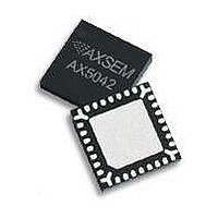
AX5043-QFN28-TU AXSEM, AX5043-QFN28-TU Datasheet - Page 35

AX5043-QFN28-TU
Manufacturer Part Number
AX5043-QFN28-TU
Description
RF Transceiver Narrow-Band-IC
Manufacturer
AXSEM
Datasheet
1.AX5043-QFN28-TU.pdf
(60 pages)
Specifications of AX5043-QFN28-TU
Number Of Receivers
1
Number Of Transmitters
1
Wireless Frequency
70 MHz to 1050 MHz
Interface Type
SPI
Output Power
18 dBm to 22 dBm
Operating Supply Voltage
1.8 V to 3.6 V
Maximum Operating Temperature
+ 85 C
Maximum Supply Current
60 mA
Minimum Operating Temperature
- 40 C
Modulation
ASK, FSK
Lead Free Status / RoHS Status
Lead free / RoHS Compliant
5.16. Serial Peripheral Interface (SPI)
The
MOSI, MISO and SEL.
peripheral interface in all device modes.
When the interface signal SEL is pulled low, a configuration data stream is expected on the input
signal pin MOSI, which is interpreted as D0...Dx, A0...Ax, R_N/W. Data read from the interface
appears on MISO.
Figure 6 shows a write/read access to the interface. The data stream is built of an address byte
including read/write information and a data byte. Depending on the R_N/W bit and address bits
A[6..0], data D[7..0] can be written via MOSI or read at the pin MISO. R_N/W = 0 means read mode,
R_N/W = 1 means write mode.
Most registers are 8 bits wide and accessed using the waveforms as detailed in Figure 7. The most
important registers are at the beginning of the address space, i.e. at addresses less than 0x70.
These registers can be accessed more efficiently using the short address form, which is detailed in
Figure 6.
Some registers are longer than 8 bits. These registers can be accessed more quicly than by reading
and writing individual 8 bit parts. This is illustrated in Figure 8. Accesses are not limited by 16 bits
either, reading and writing data bytes can be continued as long as desired. After each byte, the
address counter is incremented by one. Also, this access form works with long addresses.
During the address phase of the access, the
feature is designed to speed up the software decision on what to do in an interrupt handler.
The status bits contain the following information:
Note: Bit cells 8-15 (S7…S0) are only available in two address byte SPI access formats.
Version 0.2
SPI bit
cell
10
11
12
13
14
15
0
1
2
3
4
5
6
7
8
9
AX5043
Status
-
S14
S13
S12
S11
S10
S9
S8
S7
S6
S5
S4
S3
S2
S1
S0
can be programmed via a four wire serial interface according SPI using the pins CLK,
Meaning / Register Bit
1 (when transitioning out of deep sleep mode, this bit transitions from 0 ! 1 when the
power becomes ready)
PLL LOCK
FIFO OVER
FIFO UNDER
FIFO FULL
FIFO EMPTY
FIFOSTAT(1)
FIFOSTAT(0£)
PWRGOOD (not BROWNOUT)
PWR INTERRUPT PENDING
RADIO EVENT PENDING
XTAL OSCILLATOR RUNNING
WAKEUP INTERRUPT PENDING
LPOSC INTERRUPT PENDING
GPADC INTERRUPT PENDING
DSP INTERFACE INTERRUPT PENDING
Registers for setting up the
Preliminary
AX5043 outputs the most important status bits. This
AX5043
are programmed via the serial
Circuit Description
Datasheet AX5043
35


