SF2001E RFM, SF2001E Datasheet
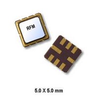
SF2001E
Specifications of SF2001E
Available stocks


Related parts for SF2001E


SF2001E Summary of contents
Page 1
... MHz SAW Filter Units dBm VDC °C °C SM3030-6 Min Typ Max 1960 2.35 4.0 1.4 2.4 20.0 32.0 10.0 21.0 4.5 10.0 20.0 50 22.0 29.0 10.0 15.0 1.7 2 -30 +80 652 YWWS SF2001E - 7/21/10 Units MHz Ω Ω °C Page ...
Page 2
... Frequency Characteristics: www.RFM.com E-mail: info@rfm.com ©2009-2010 by RF Monolithics, Inc. Page SF2001E - 7/21/10 ...
Page 3
... Reflections Functions: S11 VSWR S22 VSWR www.RFM.com E-mail: info@rfm.com ©2009-2010 by RF Monolithics, Inc. Page SF2001E - 7/21/10 ...
Page 4
... Materials 0.3 to 1.0 µm Gold over 1.27 to 8.89 µm Nickel 2.0 to 3.0 µm Nickel Al O Ceramic Free Bottom View Max 0.123 0.123 0.054 0.040 0.115 0.068 0.038 0.064 0.029 0.056 Page SF2001E - 7/21/10 ...
Page 5
... SECTION A-A www.RFM.com E-mail: info@rfm.com ©2009-2010 by RF Monolithics, Inc. Inches 12.0 2.0 COMPONENT ORIENTATION 2.0 4 3.35 8.0 SECTION B-B “B” Quantity Per Reel millimeters 7 178 500 13 330 3000 A 1.5 A R0.5 (TYP.) 1.5 USER DIRECTION OF FEED Page SF2001E - 7/21/10 ...