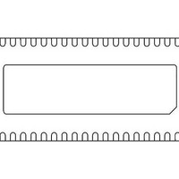
MAX4936CTN+ Maxim Integrated Products, MAX4936CTN+ Datasheet

MAX4936CTN+
Specifications of MAX4936CTN+
Related parts for MAX4936CTN+
MAX4936CTN+ Summary of contents
Page 1
... All devices are available in a small, 56-pin, 5mm x 11mm TQFN package, and are specified over the commercial 0NC to +70NC temperature range. LOW-VOLTAGE PART ISOLATION Yes MAX4936CTN+ No MAX4937CTN+ Yes MAX4938CTN+** No MAX4939CTN+** +Denotes a lead(Pb)-free/RoHS-compliant package. *EP = Exposed pad. ...
Page 2
Octal High-Voltage Transmit/Receive Switches ABSOLUTE MAXIMUM RATINGS (All voltages referenced to GND, unless otherwise noted.) V Positive Supply Voltage ...................................-0. LVCC_ Positive Supply Voltage ....................-0. LVEE_ Negative Supply Voltage ....................-6V ...
Page 3
Octal High-Voltage Transmit/Receive Switches ELECTRICAL CHARACTERISTICS (continued +1.62V to +5.5V +2.7V to +5.5V unless otherwise noted. Typical values are at T PARAMETER SYMBOL HV_ Off-Leakage Current I COM_ Off-Leakage Current I LCOM_ NO_ ...
Page 4
Octal High-Voltage Transmit/Receive Switches ELECTRICAL CHARACTERISTICS (continued +1.62V to +5.5V +2.7V to +5.5V unless otherwise noted. Typical values are at T PARAMETER SYMBOL 2nd Harmonic Distortion 3rd Harmonic Distortion Two-Tone Intermodulation Distortion (Note ...
Page 5
Octal High-Voltage Transmit/Receive Switches ELECTRICAL CHARACTERISTICS (continued +1.62V to +5.5V +2.7V to +5.5V unless otherwise noted. Typical values are at T PARAMETER SYMBOL Positive Logic Supply Current Positive Analog Supply Current Positive Analog ...
Page 6
Octal High-Voltage Transmit/Receive Switches D DIN CLK DOUT OFF T/R SWITCH ON CLR 50% Figure 1. Serial Interface Timing 6 ______________________________________________________________________________________ D 50% 50% N 50 ...
Page 7
Octal High-Voltage Transmit/Receive Switches (V = +3V +5V -5V wise noted I SUPPLY CURRENT 2.0 ONE CHANNEL ON 1.5 1.0 ...
Page 8
Octal High-Voltage Transmit/Receive Switches (V = +3V +5V -5V wise noted.) PSRR vs. FREQUENCY - 200Ω NO_ R = 200Ω COM_ PSRR_V EE -75 -80 PSRR_V CC -85 1 ...
Page 9
Octal High-Voltage Transmit/Receive Switches TOP VIEW NO1 49 LVCC1 CLR 52 GND 53 N.C. 54 COM1 55 HV1 NO1 49 ...
Page 10
Octal High-Voltage Transmit/Receive Switches PIN NAME MAX4936/ MAX4937/ MAX4938 MAX4939 15, 18, 54 13, 15, 16, 18, 19, 21, 54 COM3 5 — COM4 8 — ...
Page 11
Octal High-Voltage Transmit/Receive Switches PIN NAME MAX4936/ MAX4937/ MAX4938 MAX4939 24 24 CLK 25 25 DIN 26 26 DOUT 27 27 LVCC8 28 28 NO8 29 29 LVEE8 30 30 LVCC7 31 31 NO7 32 32 LVEE7 33 33 LVCC6 ...
Page 12
Octal High-Voltage Transmit/Receive Switches PIN NAME MAX4936/ MAX4937/ MAX4938 MAX4939 41 41 LVCC4 42 42 LVEE3 LVCC3 45 45 LVEE2 LVCC2 48 48 LVEE1 LVCC1 ...
Page 13
Octal High-Voltage Transmit/Receive Switches Functional Diagram V DD MAX4936−MAX4939 (SINGLE CHANNEL) * HV_ COM_ V CC LVEE_ SPI LOGIC GND CLK DIN DOUT LE CLR *LOW-VOLTAGE ISOLATION DIODES AVAILABLE ON MAX4936/MAX4938 ONLY. **OUTPUT CLAMP DIODES AVAILABLE ON MAX4936/MAX4937 ONLY. Detailed ...
Page 14
Octal High-Voltage Transmit/Receive Switches LVCC (LVEE DIODE BRIDGE Figure 3. Diode Bias Current Control LE CLK DIN D11 MSB D11' DOUT Figure 4. Latch-Enable Interface Timing 14 _____________________________________________________________________________________ Drive CLR logic-high to reset the ...
Page 15
Octal High-Voltage Transmit/Receive Switches Table 1. Serial Interface Programming DATA BITS (LSB ...
Page 16
Octal High-Voltage Transmit/Receive Switches Applications Information For medical ultrasound applications, see Figures 5, 6, and 7. Ultrasound-Specific IMD3 Specification Unlike typical communications applications, the two input tones are not equal in magnitude for the ultrasound-spe- cific IMD3 two-tone specification. In ...
Page 17
Octal High-Voltage Transmit/Receive Switches TRANSDUCERS HV MUX HV MUX HV MUX CONNECTORS Figure 6. Ultrasound T/R Path with One Transmit per Receive Channel and External Isolation (One Channel Only) TRANSDUCERS HV MUX HV RELAY MUX MUX HV MUX CONNECTORS Figure ...
Page 18
Octal High-Voltage Transmit/Receive Switches Figure 8. Ultrasound IMD3 Measurement Technique DIN CLK LE CLR Figure 9. Interfacing Multiple Devices by Daisy-Chaining Chip Information PROCESS: BCDMOS 18 _____________________________________________________________________________________ Application Diagrams (continued) ULTRASOUND IMD3 F1 - ( ...
Page 19
... Maxim cannot assume responsibility for use of any circuitry other than circuitry entirely embodied in a Maxim product. No circuit patent licenses are implied. Maxim reserves the right to change the circuitry and specifications without notice at any time. Maxim Integrated Products, 120 San Gabriel Drive, Sunnyvale, CA 94086 408-737-7600 2011 Maxim Integrated Products © ...


