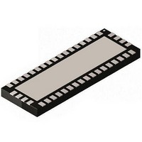
MAX14978ETO+ Maxim Integrated Products, MAX14978ETO+ Datasheet

MAX14978ETO+
Specifications of MAX14978ETO+
Related parts for MAX14978ETO+
MAX14978ETO+ Summary of contents
Page 1
... SuperSpeed Analog Switches Low Quiescent Current: 36µA (typ) S All Link Training is Preserved (SuperSpeed) S LVCMOS Control (1. Operation from a Single +3.3V Power Supply S Small, 3.5mm x 9.0mm, 42-Pin TQFN Package S PART MAX14978ETO+ +Denotes a lead(Pb)-free/RoHS-compliant package. *EP = Exposed pad. +3.3V 0.1µF SEL1 SEL2 NCD+ NCD- ...
Page 2
SuperSpeed USB Passive Switch (Low/Full/Hi/SuperSpeed) ABSOLUTE MAXIMUM RATINGS (All voltages referenced to GND, unless otherwise noted.) V .......................................................................-0.3V to +6. .......................................................................-0.3V to +4.0V DD SEL1, EN, COMD_, NOD_, NCD_ (Note 1) ...................................... -0. SEL2, COM0_, COM1_, ...
Page 3
ELECTRICAL CHARACTERISTICS (continued +3.0V to +5.5V +3.0V to +3.6V +25NC.) (Note 2) A PARAMETER SYMBOL On-Resistance Match Between DR Channels On-Resistance Match Between DR Pairs of Same Channels On-Resistance Flatness R ...
Page 4
SuperSpeed USB Passive Switch (Low/Full/Hi/SuperSpeed) ELECTRICAL CHARACTERISTICS (continued +3.0V to +5.5V +3.0V to +3.6V +25NC.) (Note 2) A PARAMETER SYMBOL Crosstalk (Note 7) Signaling Data Rate LOGIC INPUT Input Logic-High Input ...
Page 5
ELECTRICAL CHARACTERISTICS (continued +3.0V to +5.5V +3.0V to +3.6V +25NC.) (Note 2) A PARAMETER SYMBOL Fault-Protection Recovery Time C NO(OFF) NO_ or NC_ Off-Capacitance C NC(OFF) COM_ Off-Capacitance C COM(OFF) COM_ ...
Page 6
SuperSpeed USB Passive Switch (Low/Full/Hi/SuperSpeed 0.1 µ F 0.1 µ SEL_ DD NC_ MAX14978 50Ω GND MEASUREMENTS ARE STANDARDIZED AGAINST SHORTS AT IC TERMINALS. OFF-ISOLATION IS MEASURED BETWEEN ...
Page 7
F NO_ NC_+ IN+ NO_ NC_- IN- +1.5V V IN+ 50% 0V +1.5V V 50% IN PLHX +1.5V V OUT+ 50% 0V +1.5V 50% V OUT PHLY Figure ...
Page 8
SuperSpeed USB Passive Switch (Low/Full/Hi/SuperSpeed +3. COMD_ FPR NOD_ V NCD_ Figure 4. Fault Protection Response/Recovery Time ( 3.3V +25NC, unless otherwise noted ...
Page 9
V = 3.3V +25NC, unless otherwise noted SUPERSPEED HI-SPEED SWITCHES SUPPLY CURRENT vs. TEMPERATURE +3. -40 - TEMPERATURE ...
Page 10
SuperSpeed USB Passive Switch (Low/Full/Hi/SuperSpeed) TOP VIEW N.C. N.C. N.C. N.C. PIN NAME 36, N.C. No Connection. Not internally connected. 39-42 4 COMD+ Hi-Speed USB Analog Switch, Common D+ Terminal 5, 10, 14, GND Ground ...
Page 11
SuperSpeed USB Passive Switch PIN NAME Active-Low Enable Input for Hi-Speed USB Switches. Drive EN high to put Hi-Speed USB switches high impedance. Drive EN low for normal operation. Positive-Supply Voltage Input for Hi-Speed USB Switches. Bypass ...
Page 12
SuperSpeed USB Passive Switch (Low/Full/Hi/SuperSpeed) Detailed Description The MAX14978 is ideal for SuperSpeed USB and low/ full/Hi-Speed (1.5/12/480Mbps) USB switching applica- tions. The low V threshold of the device permits used with logic levels as low ...
Page 13
ESD Test Conditions ESD performance depends on a variety of conditions. Contact Maxim for a reliability report that documents test setup, test methodology, and test results. Human Body Model Figure 6a shows the Human Body Model, and Figure 6b shows ...
Page 14
SuperSpeed USB Passive Switch (Low/Full/Hi/SuperSpeed) Power-Supply Sequencing Caution: Do not exceed the absolute maximum rat- ings because stresses beyond the listed ratings may cause permanent damage to the device. Proper power-supply sequencing is recommended for all CMOS devices. Always apply ...
Page 15
... Maxim cannot assume responsibility for use of any circuitry other than circuitry entirely embodied in a Maxim product. No circuit patent licenses are implied. Maxim reserves the right to change the circuitry and specifications without notice at any time. Maxim Integrated Products, 120 San Gabriel Drive, Sunnyvale, CA 94086 408-737-7600 2010 Maxim Integrated Products © ...


