BGA 758L7 E6327 Infineon Technologies, BGA 758L7 E6327 Datasheet
BGA 758L7 E6327
Specifications of BGA 758L7 E6327


Related parts for BGA 758L7 E6327


BGA 758L7 E6327 Summary of contents
Page 1
5-6 GHz LNA for WLAN Revision 1.0, 2010-02-22 Preliminary R F & ...
Page 2
... Infineon Technologies Office. Infineon Technologies components may be used in life-support devices or systems only with the express written approval of Infineon Technologies failure of such components can reasonably be expected to cause the failure of that life-support device or system or to affect the safety or effectiveness of that device or system. Life support devices or systems are intended to be implanted in the human body or to support and/or maintain and sustain and/or protect human life ...
Page 3
... New document layout Electrical Characteristics adjusted Trademarks of Infineon Technologies AG A-GOLD™, BlueMoon™, COMNEON™, CONVERGATE™, COSIC™, C166™, CROSSAVE™, CanPAK™, CIPOS™, CoolMOS™, CoolSET™, CONVERPATH™, CORECONTROL™, DAVE™, DUALFALC™, DUSLIC™, EasyPIM™ ...
Page 4
Table of Contents Table of Contents . . . . . . . . . . . . . . . . . . . . . . . . . . . . . . . . . . ...
Page 5
List of Figures Figure 1 Block Diagram . . . . . . . . . . . . . . . . . . . . . . . . . . . . . . . . . ...
Page 6
List of Tables Table 1 Pin Definition and Function . . . . . . . . . . . . . . . . . . . . . . . . . . . . . . . ...
Page 7
GHz LNA for WLAN Features 2 S • Gain 12 5.5 GHz 21 P • High Linearity, Input = -3.5 dBm at 5.5 GHz -1dB NF • Low noise figure ...
Page 8
Description The BGA758L7 GHz Silicon Germanium low noise amplifier MMIC in tiny TSLP-7-8 package. The LNA delivers a gain of 12.5 dB while giving an excellent noise figure of 1 the application configuration ...
Page 9
Maximum Ratings Table 2 Maximum Ratings Parameter Voltage at pin VCC Voltage at pin IN Voltage at pin BIAS Voltage at pin OUT Voltage at pin PON Voltage at pin GND Current into pin VCC RF input power Total ...
Page 10
Electrical Characteristics 2.1 Electrical Parameter Table 4 Electrical Characteristics Parameter Pass band frequency range Gain Gain flatness Reverse isolation 2) Noise figure Input return loss Output return loss Input power at 1dB compression point Maximum gain out of band ...
Page 11
Digital Signals Table 5 Digital Control Parameter Parameter Power on control voltage range Control voltage for power on Control voltage for power off Capacitance at power on pin Input current at power on pin Preliminary Data Sheet Symbol Values ...
Page 12
Application Information Application Board Configuration PON RFin Figure 2 Application Schematic Table 6 Bill of Materials Name Value list of all application notes is available at http://goto.infineon.com/smallsignaldiscretes-appnotes. Preliminary ...
Page 13
Figure 3 Drawing of Application Board Micro- Via 150 µm Figure 4 Cross-section of Application Board Preliminary Data Sheet Via 500 µm Rogers 4003 200 µm Core FR4 800 µm BGA 758L7 _Cross_section.vsd 13 BGA758L7 Application Information TOP- Layer CU ...
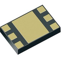
Page 14
Package Information Top view Pin 1 marking 1) Dimension applies to plated terminals 2) Dimension of 0.02 MIN. is guaranteed Figure 5 Package Outline TSLP-7-8 (side and bottom view) Figure 6 Marking Layout (top view) Preliminary Data Sheet Bottom ...
Page 15
Copper Figure 7 Footprint TSLP-7-8 Preliminary Data Sheet SMD 0.25 0.23 Solder mask Vias 15 BGA758L7 Package Information 1.21 0.51 0.25 0.25 0.23 0.25 0.23 Stencil apertures TSLP-7-8-FP V01 Revision 1.0, 2010-02-22 ...
Page 16
... Published by Infineon Technologies AG ...