DR3000 RFM, DR3000 Datasheet - Page 4
DR3000
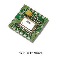
Manufacturer Part Number
DR3000
Description
RF Modules & Development Tools Transceiver Module 2G, 916.5MHz 2.4kbps
Manufacturer
RFM
Datasheet
1.DR3000.pdf
(5 pages)
Specifications of DR3000
Lead Free Status / RoHS Status
Lead free / RoHS Compliant


www.RFM.com
©2008 by RF Monolithics, Inc.
Pin
10
12
13
14
11
8
9
LPF ADJ
RF GND
Name
CTR1
CTR0
RFIO
GND
VCC
E-mail: info@rfm.com
2.4 kbps Application Circuit
13
14
12
1
This pin is the receiver low-pass filter bandwidth adjust, and is connected directly to the transceiver LPFADJ pin. R6 on the cir-
cuit board (330 K) is connected between LPFADJ and ground will be in parallel with any external resistor connected to LPF
ADJ. The filter bandwidth is set by the parallel resistance of R6 and the external resistor (if used). The equivalent resistor value
can range from 330 K to 820 ohms, providing a filter 3 dB bandwidth f
determined by:
f
A ±5% resistor should be used to set the filter bandwidth. This will provide a 3 dB filter bandwidth between f
with variations in supply voltage, temperature, etc. The filter provides a three-pole, 0.05 degree equiripple phase response. The
peak drive current available from RXDATA increases in proportion to the filter bandwidth setting. As shipped, the transceiver
module is set up for nominal 2.4 kbps operation. An external resistor can be added between Pin 6 and ground to support higher
data rates. Preamble training times will not be decreased, however, unless C3 is replaced with a smaller capacitor value (see
the descriptions of Pins 2 and 3 above). Refer to sections 1.4.3, 2.5.1 and 2.6.1 in the ASH Transceiver Designer’s Guide for
additional information on data rate adjustments.
This is the positive supply voltage pin for the module. The operating voltage range is 2.7 to 3.5 Vdc. It is also possible to use
Pin 1 as the Vcc input. Please refer to the Pin 1 description above.
This is the supply voltage return pin.
CTR1 is connected to the CNTRL1 control pin on the transceiver. CTR1 and CTR0 select the transceiver operating modes.
CTR1 and CTR0 both high place the unit in the receive mode. CTR1 and CTR0 both low place the unit in the power-down
(sleep) mode. CTR1 high and CTR0 low place the unit in the ASK transmit mode. CTR1 low and CTR0 high place the unit in
the OOK transmit mode. CTR1 is a high-impedance input (CMOS compatible). This pin must be held at a logic level; it cannot
be left unconnected. At turn on, the voltage on this pin and CTR0 should rise with VCC until VCC reaches 2.7 Vdc (receive
mode). Thereafter, any mode can be selected.
CTR0 is connected to the CNTRL0 control pin on the transceiver CTR0 is used with CTR1 to control the operating modes of
the transceiver. CTR0 is a high-impedance input (CMOS compatible). This pin must be held at a logic level; it cannot be left
unconnected. At turn on, the voltage on this pin and CTR1 should rise with VCC until VCC reaches 2.7 Vdc (receive mode).
Thereafter, any mode can be selected.
RFIO is the RF input/output pin. A matching circuit for a 50 ohm load (antenna) is implemented on the circuit board between
this pin and the transceiver SAW filter transducer.
This pin is the RF ground (return) to be used in conjunction with the RFIO pin. For example, when connecting the transceiver
module to an external antenna, the coaxial cable ground is connected this pin and the coaxial cable center conductor is con-
nected to RFIO.
LPF
R/T
11
2
= 1445/ (330*R
DR3000
10
3
3 Vdc
9
4
LPF
8
5
3.3 K
7
6
/(330 + R
LPF
Data In
Data Out
)), where R
LPF
is in kilohms, and f
Description
LPF
LPF
19.2 kbps Application Circuit
from 4.4 kHz to 1.8 MHz. The 3 dB filter bandwidth is
is in kHz
13
14
12
1
R/T
11
2
DR3000
10
3
3 Vdc
9
4
8
5
3.3 K
7
6
LPF
and 1.3* f
DR3000 - 4/8/08
Data In
Data Out
Page 4 of 5
LPF
Related parts for DR3000
Image
Part Number
Description
Manufacturer
Datasheet
Request
R

Part Number:
Description:
RF Modules & Development Tools TRC105 Evaluation Board 447-451 MHz
Manufacturer:
RFM
Datasheet:
Part Number:
Description:
RF Modules & Development Tools TRC105 Evaluation Board 365-381 MHz
Manufacturer:
RFM
Datasheet:
Part Number:
Description:
RF Modules & Development Tools TRC105 Evaluation Board 303-307 MHz
Manufacturer:
RFM
Datasheet:
Part Number:
Description:
RF Modules & Development Tools TRC105 Evaluation Board 382-398 MHz
Manufacturer:
RFM
Datasheet:
Part Number:
Description:
RF Modules & Development Tools TRC105 Evaluation Board 416-436 MHz
Manufacturer:
RFM
Datasheet:
Part Number:
Description:
RF Modules & Development Tools TRC105 Evaluation Board 342-348 MHz
Manufacturer:
RFM
Datasheet:
Part Number:
Description:
RF Modules & Development Tools TRC105 Evaluation Board 402-407 MHz
Manufacturer:
RFM
Datasheet:
Part Number:
Description:
RF Modules & Development Tools TRC105 Evaluation Board 310-319 MHz
Manufacturer:
RFM
Datasheet:

Part Number:
Description:
RF Modules & Development Tools TXC101 Development Kit 310-319 MHz
Manufacturer:
RFM
Part Number:
Description:
RF Modules & Development Tools TXC102 Development Kit 430-439 MHz
Manufacturer:
RFM


Part Number:
Description:
10-Terminal Ceramic Surface-Mount Case 7 x 5 mm Nominal Footprint
Manufacturer:
RFM [RF Monolithics, Inc]
Datasheet:
Part Number:
Description:
QUAD-BAND GSM850/GSM/DCS/PCS POWER AMP MODULE
Manufacturer:
RFM [RF Monolithics, Inc]
Datasheet:
Part Number:
Description:
402 to 405 MHz Medical Band Front-end Filter
Manufacturer:
RFM [RF Monolithics, Inc]
Datasheet:
Part Number:
Description:
674.03 MHz SAW Resonator
Manufacturer:
RFM [RF Monolithics, Inc]
Datasheet: