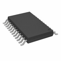
ADF7901BRU Analog Devices Inc, ADF7901BRU Datasheet

ADF7901BRU
Specifications of ADF7901BRU
Available stocks
Related parts for ADF7901BRU
ADF7901BRU Summary of contents
Page 1
FEATURES Single-chip, low power UHF transmitter 369.5 MHz to 395.9 MHz frequency operation using fractional-N PLL and fully integrated VCO 3.0 V supply voltage Data rates kbps supported Low current consumption dBm output ...
Page 2
ADF7901 TABLE OF CONTENTS Features .............................................................................................. 1 General Description ......................................................................... 1 Functional Block Diagram .............................................................. 1 Specifications..................................................................................... 3 Absolute Maximum Ratings............................................................ 5 ESD Caution.................................................................................. 5 Pin Configuration and Function Descriptions............................. 6 Typical Performance Characteristics ............................................. 8 Circuit Description........................................................................... 9 Loop ...
Page 3
SPECIFICATIONS V =3.0 V; GND = MIN MAX Table 1. Parameter RF CHARACTERISTICS Output Frequency Ranges Channel 1 Channel 2 Channel 3 Channel 4 Channel 5 Channel 6 Channel 7 Channel ...
Page 4
ADF7901 Parameter PHASE-LOCKED LOOP VCO Gain 3, 7 Spurious Integer Boundary Reference 3 Harmonics Second Harmonic Third Harmonic All Other Harmonics REFERENCE INPUT Crystal Reference 8 Crystal ESR POWER AMPLIFIER ...
Page 5
ABSOLUTE MAXIMUM RATINGS 25°C, unless otherwise noted. A Table 2. Parameter Value GND −0 +4 RFVDD to GND −0 +4.0 V Digital I/O Voltage to GND −0.3 V ...
Page 6
ADF7901 PIN CONFIGURATION AND FUNCTION DESCRIPTIONS Table 3. Pin Function Descriptions Pin No. Mnemonic Function 1 DV Positive Supply for the Digital Circuitry. This must be 3.0 V. Decoupling capacitors to the analog ground plane DD should be placed as ...
Page 7
Pin No. Mnemonic Function 21 DV Voltage Supply for VCO and PA Section. It should be supplied with 3.0 V. Decoupling capacitors to the ground DD plane should be placed as close as possible to this pin. 22 PA_EN This ...
Page 8
ADF7901 TYPICAL PERFORMANCE CHARACTERISTICS RSET Figure 3. Output Power vs. R FSK, Upper FSK Channels, SET Measured into 50 Ω ...
Page 9
CIRCUIT DESCRIPTION Table 4. Frequency (MHz) FSK3 FSK2 369 371 375 376 384.0 Don’t Don’t care care 388 391 394 395 LOOP FILTER The ...
Page 10
ADF7901 22nF C VCO R 3.6kΩ VCO IN CP TxDATA FSK1 FSK2 FSK3 OOK_SEL PA_EN Figure 8. Applications Diagram for the ADF7901 in a Remote Control System LAYOUT GUIDELINES The layout of the board is crucial to ensuring low levels ...
Page 11
... OUTLINE DIMENSIONS 0.15 0.05 ORDERING GUIDE Model Temperature Range ADF7901BRU 0°C to 50°C ADF7901BRU-REEL 0°C to 50°C ADF7901BRU-REEL7 0°C to 50°C 1 ADF7901BRUZ 0°C to 50°C 1 ADF7901BRUZ-RL 0°C to 50°C 1 ADF7901BRUZ-RL7 0°C to 50°C EVAL-ADF7901EB Pb-free part. 7.90 7.80 7. 4.50 4.40 4.30 6 ...
Page 12
ADF7901 NOTES ©2006 Analog Devices, Inc. All rights reserved. Trademarks and registered trademarks are the property of their respective owners. D05349-0-3/06(A) Rev Page ...


