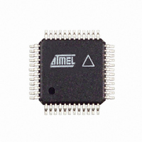
AT86RF211SAH-R Atmel, AT86RF211SAH-R Datasheet - Page 28

AT86RF211SAH-R
Manufacturer Part Number
AT86RF211SAH-R
Description
IC RF TXRX FSK 400-950MHZ 48TQFP
Manufacturer
Atmel
Datasheet
1.AT86RF211SDK.pdf
(66 pages)
Specifications of AT86RF211SAH-R
Frequency
400MHz ~ 950MHz
Data Rate - Maximum
100kbps
Modulation Or Protocol
FSK
Applications
ISM
Power - Output
7dBm ~ 12dBm
Sensitivity
-107dBm
Voltage - Supply
2.4 V ~ 3.6 V
Data Interface
PCB, Surface Mount
Antenna Connector
PCB, Surface Mount
Operating Temperature
-40°C ~ 85°C
Package / Case
48-TQFP Exposed Pad, 48-eTQFP, 48-HTQFP, 48-VQFP
Lead Free Status / RoHS Status
Contains lead / RoHS non-compliant
Memory Size
-
Current - Transmitting
-
Current - Receiving
-
2.3
2.3.1
2.3.1.1
2.3.1.2
28
Digital Features
AT86RF211S
Clock Recovery Function
Preamble
Algorithm Overview
The clock recovery algorithm in the AT86RF211S has been improved and the new algo-
rithm must be used. To use the new algorithm:
1. Put the device into RF211S mode: ADDFEAT = CTRL1[0] = 1
2. Select the improved algorithm by setting bit NEWDATACLK = DTR[13] = 1
For compatibility purposes only, it is nevertheless possible to run the former algorithm,
(the algorithm of the AT86RF211). This algorithm is automatically activated in the
RF211 mode or if bit NEWDATACLK is kept in reset state in RF211S mode.
It is now possible, in RF211S mode only, to inhibit the clock recovery when RSSI is too
low, leaving the MCU in sleep mode. This is performed by the DATACLKEN bit in the
DTR register.
The clock recovery function is activated by setting the DATACLK bit of the CTRL1 regis-
ter to 1.
The clock recovery function provides the data clock on the DATACLK pin, synchronized
on the received data flow. The targeted position for the rising edge of the clock is the
middle of the data bit, eliminating synchronization problems and facilitating readout by
the microcontroller.
The clock’s recovery mechanism is based on the generation of a basic data clock with a
period given by the DATARATE of CTRL2 with a step of approximately 100 ns. This
basic clock is synchronized on the received data flow. The phase correction step is fixed
by DATATOL of the CTRL2 register (steps of approximately 100 ns also).
Therefore, DATATOL can:
The best DATATOL value is a a balance of the above three points.
If the tolerance is too high, the rate value is reached earlier, and could be unstable (too
big a step).
If the tolerance is too low, it could be difficult to catch up with the data and the function
may be lost.
The tolerance is able to compensate for the difference of datarate generators between
Rx and Tx.
The synchronization mechanism is explained by the chronogram in Figure 2-25. Syn-
chronization is done for the first bit. In worst case scenarios, when the data and clock
arrive at the same time, synchronization begins at the second bit. Notice that the DATA-
• Compensate for the difference between the read data rates from the transmitter and
• Allow fast initial synchronization of the data clock, avoiding bit transition times, and
• Keep the appropriate data rate (no additional and no removed bit) when noisy data
the receiver (fixed by DATARATE).
converge towards the middle of the bit.
with a bad bit transition position arrives.
5348B–WIRE–03/06


