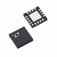
LT5522EUF Linear Technology, LT5522EUF Datasheet

LT5522EUF
Specifications of LT5522EUF
Available stocks
Related parts for LT5522EUF
LT5522EUF Summary of contents
Page 1
... The LT5522 delivers high performance and small size without excessive power consumption. , LTC and LT are registered trademarks of Linear Technology Corporation. All other trademarks are the property of their respective owners. *Operation over a wider frequency range is possible with reduced performance. ...
Page 2
... CC 16-LEAD (4mm × 4mm) PLASTIC QFN EXPOSED PAD (PIN 17) IS GND, MUST BE SOLDERED TO PCB ORDER PART NUMBER LT5522EUF Order Options Tape and Reel: Add #TR Lead Free: Add #PBF Lead Free Tape and Reel: Add #TRPBF Lead Free Part Marking: Consult LTC Marketing for parts specified with wider operating temperature ranges. ...
Page 3
AC ELECTRICAL CHARACTERISTICS = –7dBm (–7dBm/tone for 2-tone IIP3 tests, ∆f = 1MHz 25° 140MHz, unless otherwise noted. (Notes 2, 3) (Test circuit shown in Figure 2). PARAMETER Conversion Gain Conversion Gain vs Temperature ...
Page 4
LT5522 W U TYPICAL AC PERFOR A CE CHARACTERISTICS = –7dBm (–7dBm/tone for 2-tone IIP3 tests, ∆f = 1MHz 5V High 25° 140MHz, unless otherwise noted. (Test circuit ...
Page 5
W U TYPICAL AC PERFOR A CE CHARACTERISTICS (L3 = 3.9nH 5V High 25° measured at 140MHz, unless otherwise noted. (Test circuit shown in Figure 2). Low Band Conv Gain, IIP3 ...
Page 6
LT5522 W U TYPICAL AC PERFOR A CE CHARACTERISTICS = 1150MHz at –12dBm (–12dBm/tone for 2-tone IIP3 tests, ∆f = 1MHz), LO swept from 1200MHz 5V High 25° 2200MHz, ...
Page 7
W U TYPICAL AC PERFOR A CE CHARACTERISTICS from Pin 5V High 25° measured at 140MHz, unless otherwise noted. (Test circuit shown in Figure 2) Conv Gain, IIP3 and SSB ...
Page 8
LT5522 CTIO S NC (Pins 13, 16): Not Connected Internally. These pins should be grounded on the circuit board for improved and isolation. + – RF ...
Page 9
TEST CIRCUITS LO IN 400MHz TO 2700MHz RF IN 400MHz TO 2700MHz L3 (HIGH (LOW OR BAND) OPTIONAL BAND) SHUNT REACTANCE USED FOR LOW BAND OR HIGH BAND RF MATCH ONLY REF DES VALUE SIZE PART NUMBER C1 0.01µF 0402 ...
Page 10
LT5522 U U APPLICATIO S I FOR ATIO Introduction The LT5522 consists of a high linearity double-balanced mixer, RF buffer amplifier, high speed limiting LO buffer amplifier and bias/enable circuits. The IC has been opti- mized for downconverter applications where ...
Page 11
U U APPLICATIO S I FOR ATIO RF input impedance and S11 versus frequency are shown in Table 1. The listed data is referenced to the RF + the RF pin grounded (no external matching). This infor- mation can be ...
Page 12
LT5522 U U APPLICATIO S I FOR ATIO 0 –5 –10 –15 –20 –25 –30 1E8 1E9 LO FREQUENCY (Hz) Figure 9. LO Input Return Loss Table 2. LO Port Input Impedance vs Frequency FREQUENCY INPUT (MHZ) IMPEDANCE 100 200.5 ...
Page 13
U U APPLICATIO S I FOR ATIO Higher linearity and lower LO-IF leakage can be realized by using the simple, three element lowpass matching net- work shown in Figure 10. Matching elements C4, L1 and L2 form a 400Ω to ...
Page 14
LT5522 U U APPLICATIO S I FOR ATIO C4 L1 4.7pF 100nH + 4.7pF 390nH – 1000pF 100nH V CC Figure 15. Narrowband Bridge IF Balun (240MHz Example) inductor is recommended for L4 to ...
Page 15
... SHADED AREA IS ONLY A REFERENCE FOR PIN 1 LOCATION ON THE TOP AND BOTTOM OF PACKAGE Information furnished by Linear Technology Corporation is believed to be accurate and reliable. However, no responsibility is assumed for its use. Linear Technology Corporation makes no represen- tation that the interconnection of its circuits as described herein will not infringe on existing patent rights Package 16-Lead Plastic QFN (4mm × ...
Page 16
... IIP3 at 1.9GHz 12.5dB, Single-Ended RF and LO Ports Precision V Offset Control, Adjustable Gain and Offset Voltage OUT 60dB Dynamic Range, Superb Temperature Stability, Tiny 2mm × 2mm SC70 Package, Low Power Consumption www.linear.com ● 5522fa LT 1105 REV A • PRINTED IN USA © LINEAR TECHNOLOGY CORPORATION 2003 ...


