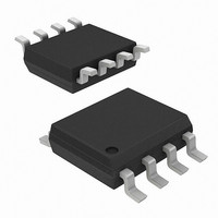
AD8313ARM Analog Devices Inc, AD8313ARM Datasheet - Page 18

AD8313ARM
Manufacturer Part Number
AD8313ARM
Description
IC LOGARTIHMIC AMP 70DB 8-MSOP
Manufacturer
Analog Devices Inc
Type
Logarithmic Ampr
Datasheet
1.AD8313ARMZ.pdf
(24 pages)
Specifications of AD8313ARM
Rohs Status
RoHS non-compliant
Frequency
100MHz ~ 2.5GHz
Rf Type
RADAR, 802.11/Wi-Fi, 8.2.16/WiMax, Wireless LAN
Input Range
-65dBm ~ 0dBm
Accuracy
±1dB
Voltage - Supply
2.7 V ~ 5.5 V
Current - Supply
13.7mA
Package / Case
8-TSSOP, 8-MSOP (0.118", 3.00mm Width)
Number Of Channels
1
Number Of Elements
8
Power Supply Requirement
Single
Voltage Gain Db
84dB
Input Resistance
0.0009@5VMohm
Input Bias Current
10@5VnA
Single Supply Voltage (typ)
3/5V
Dual Supply Voltage (typ)
Not RequiredV
Power Dissipation
200mW
Rail/rail I/o Type
Rail to Rail Output
Single Supply Voltage (min)
2.7V
Single Supply Voltage (max)
5.5V
Dual Supply Voltage (min)
Not RequiredV
Dual Supply Voltage (max)
Not RequiredV
Operating Temp Range
-40C to 85C
Operating Temperature Classification
Industrial
Mounting
Surface Mount
Pin Count
8
Package Type
MSOP
Lead Free Status / RoHS Status
Not Compliant
Available stocks
Company
Part Number
Manufacturer
Quantity
Price
Company:
Part Number:
AD8313ARM
Manufacturer:
AD
Quantity:
5 510
Company:
Part Number:
AD8313ARM
Manufacturer:
NAIS
Quantity:
5 510
Company:
Part Number:
AD8313ARM
Manufacturer:
AD
Quantity:
4 130
Part Number:
AD8313ARM
Manufacturer:
ADI/亚德诺
Quantity:
20 000
Company:
Part Number:
AD8313ARM-REEL
Manufacturer:
AD
Quantity:
5 510
Company:
Part Number:
AD8313ARM-REEL
Manufacturer:
LT
Quantity:
5 510
Part Number:
AD8313ARM-REEL
Manufacturer:
ADI/亚德诺
Quantity:
20 000
Part Number:
AD8313ARM-REEL7
Manufacturer:
ADI/亚德诺
Quantity:
20 000
Part Number:
AD8313ARMZ
Manufacturer:
ADI/亚德诺
Quantity:
20 000
Part Number:
AD8313ARMZ-REEL
Manufacturer:
ADI/亚德诺
Quantity:
20 000
AD8313
As previously discussed, a modification of the board layout
produces networks that may not perform as specified. At 2.5 GHz,
a shunt inductor is sufficient to achieve proper matching. Con-
sequently, C1 and C2 are set sufficiently high that they appear as
RF shorts.
Table 4. Recommended Values for C1, C2, and
L
Freq.
(MHz)
100
900
1900
2500
Figure 37 shows the voltage response of the 100 MHz matching
network. Note the high attenuation at lower frequencies typical
of a high-pass network.
ADJUSTING THE LOG SLOPE
Figure 38 shows how the log slope can be adjusted to an exact
value. The idea is simple: the output at the VOUT pin is attenu-
ated by the variable resistor R2 working against the internal 18 kΩ
of input resistance at the VSET pin. When R2 is 0, the attenu-
ation it introduces is 0, and thus the slope is the basic 18 mV/dB.
Note that this value varies with frequency, (Figure 10). When R2
is set to its maximum value of 10 kΩ, the attenuation from
VOUT to VSET is the ratio 18/(18 + 10), and the slope is raised
to (28/18) × 18 mV, or 28 mV/dB. At about the midpoint, the
nominal scale is 23 mV/dB. Thus, a 70 dB input range changes
the output by 70 × 23 mV, or 1.6 V.
MATCH
Figure 37. Voltage Response of 100 MHz Narrow-Band Matching Network
15
10
–5
in Figure 35
5
0
50
C
(pF)
8.9
1.5
1.5
Large
MATCH
C1
(pF)
22
3
1.5
3
1.5
390
FREQUENCY (MHz)
100
C2
(pF)
15
1000
3
1000
3
1000
390
L
(nH)
270
270
8.2
8.2
2.2
2.2
2.2
MATCH
200
Voltage
Gain(dB)
12.6
9.0
6.2
3.2
Rev. D | Page 18 of 24
As stated, the unadjusted log slope varies with frequency from
17 mV/dB to 20 mV/dB, as shown in Figure 10. By placing a
resistor between VOUT and VSET, the slope can be adjusted to
a convenient 20 mV/dB as shown in Figure 39.
Table 5 shows the recommended values for this resistor, R
Also shown are values for R
approximately 50 mV/dB. The corresponding voltage swings
for a −65 dBm to 0 dBm input range are also shown in Table 6.
Table 5. Values for R
Frequency
MHz
100
900
1900
2500
100
900
1900
2500
The value for R
The value for the Original Slope, at a particular frequency, can
be read from Figure 10. The resulting output swing is calculated
by simply inserting the New Slope value and the intercept at that
frequency (Figure 10 and Figure 13) into the general equation
for the AD8313’s output voltage:
+V
+V
+V
+V
S
S
V
R
S
S
OUT
EXT
10Ω
10Ω
R1
R3
= Slope(P
10Ω
10Ω
R1
R3
=
Figure 39. Adjusting the Log Slope to a Fixed Value
(
New
EXT
0.1µF
0.1µF
R
kV
0.953
2.00
2.55
0
29.4
32.4
33.2
26.7
0.1µF
0.1µF
EXT
Figure 38. Adjusting the Log Slope
is calculated by
Slope
IN
Original
EXT
− Intercept)
1
2
3
4
in Figure 39
−
1
2
3
4
INHI
INLO
VPOS VOUT
VPOS PWDN
Slope
mV/dB
20
20
20
20
50
50.4
49.8
49.7
Original
AD8313
INHI
INLO
VPOS VOUT
VPOS PWDN
EXT
AD8313
Slope
, which increase the slope to
COMM
VSET
COMM
VSET
Slope
8
7
6
5
V
−65 dBm to 0 dBm – V
0.44 to 1.74
0.58 to 1.88
0.70 to 2.00
0.54 to 1.84
1.10 to 4.35
1.46 to 4.74
1.74 to 4.98
1.34 to 4.57
8
7
6
5
OUT
)
×
10kΩ
Swing for Pin
R2
18
R
k
EXT
Ω
18–30mV/dB
20mV/dB
EXT
.


