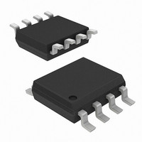
AD8313ARM Analog Devices Inc, AD8313ARM Datasheet - Page 16

AD8313ARM
Manufacturer Part Number
AD8313ARM
Description
IC LOGARTIHMIC AMP 70DB 8-MSOP
Manufacturer
Analog Devices Inc
Type
Logarithmic Ampr
Datasheet
1.AD8313ARMZ.pdf
(24 pages)
Specifications of AD8313ARM
Rohs Status
RoHS non-compliant
Frequency
100MHz ~ 2.5GHz
Rf Type
RADAR, 802.11/Wi-Fi, 8.2.16/WiMax, Wireless LAN
Input Range
-65dBm ~ 0dBm
Accuracy
±1dB
Voltage - Supply
2.7 V ~ 5.5 V
Current - Supply
13.7mA
Package / Case
8-TSSOP, 8-MSOP (0.118", 3.00mm Width)
Number Of Channels
1
Number Of Elements
8
Power Supply Requirement
Single
Voltage Gain Db
84dB
Input Resistance
0.0009@5VMohm
Input Bias Current
10@5VnA
Single Supply Voltage (typ)
3/5V
Dual Supply Voltage (typ)
Not RequiredV
Power Dissipation
200mW
Rail/rail I/o Type
Rail to Rail Output
Single Supply Voltage (min)
2.7V
Single Supply Voltage (max)
5.5V
Dual Supply Voltage (min)
Not RequiredV
Dual Supply Voltage (max)
Not RequiredV
Operating Temp Range
-40C to 85C
Operating Temperature Classification
Industrial
Mounting
Surface Mount
Pin Count
8
Package Type
MSOP
Lead Free Status / RoHS Status
Not Compliant
Available stocks
Company
Part Number
Manufacturer
Quantity
Price
Company:
Part Number:
AD8313ARM
Manufacturer:
AD
Quantity:
5 510
Company:
Part Number:
AD8313ARM
Manufacturer:
NAIS
Quantity:
5 510
Company:
Part Number:
AD8313ARM
Manufacturer:
AD
Quantity:
4 130
Part Number:
AD8313ARM
Manufacturer:
ADI/亚德诺
Quantity:
20 000
Company:
Part Number:
AD8313ARM-REEL
Manufacturer:
AD
Quantity:
5 510
Company:
Part Number:
AD8313ARM-REEL
Manufacturer:
LT
Quantity:
5 510
Part Number:
AD8313ARM-REEL
Manufacturer:
ADI/亚德诺
Quantity:
20 000
Part Number:
AD8313ARM-REEL7
Manufacturer:
ADI/亚德诺
Quantity:
20 000
Part Number:
AD8313ARMZ
Manufacturer:
ADI/亚德诺
Quantity:
20 000
Part Number:
AD8313ARMZ-REEL
Manufacturer:
ADI/亚德诺
Quantity:
20 000
AD8313
INPUT COUPLING
The signal can be coupled to the AD8313 in a variety of ways.
In all cases, there must not be a dc path from the input pins to
ground. Some of the possibilities include dual-input coupling
capacitors, a flux-linked transformer, a printed circuit balun,
direct drive from a directional coupler, or a narrow-band
impedance matching network.
Figure 32 shows a simple broadband resistive match. A
termination resistor of 53.6 Ω combines with the internal input
impedance of the AD8313 to give an overall resistive input
impedance of approximately 50 Ω. It is preferable to place the
termination resistor directly across the input pins, INHI to
INLO, where it lowers the possible deleterious effects of dc
offset voltages on the low end of the dynamic range. At low
frequencies, this may not be quite as beneficial, since it requires
larger coupling capacitors. The two 680 pF input coupling
capacitors set the high-pass corner frequency of the network at
9.4 MHz.
The high-pass corner frequency can be set higher according to
the equation
where:
In high frequency applications, the use of a transformer, balun,
or matching network is advantageous. The impedance matching
characteristics of these networks provide what is essentially a
gain stage before the AD8313 that increases the device sensitivity.
This gain effect is explored in the following matching example.
Figure 33 and Figure 34 show device performance under these
three input conditions at 900 MHz and 1.9 GHz.
While the 900 MHz case clearly shows the effect of input
matching by realigning the intercept as expected, little
improvement is seen at 1.9 GHz. Clearly, if no improvement
in sensitivity is required, a simple 50 Ω termination may be
the best choice for a given design based on ease of use and
cost of components.
50Ω SOURCE
C
f
3
dB
=
Figure 32. A Simple Broadband Resistive Input Termination
C1
C1
=
2
×
×
50Ω
×
C2
C2
π
×
1
C
×
50
680pF
680pF
C1
C2
R
53.6Ω
MATCH
AD8313
C
IN
R
IN
Rev. D | Page 16 of 24
NARROW-BAND LC MATCHING EXAMPLE
AT 100 MHz
While numerous software programs provide an easy way to
calculate the values of matching components, a clear under-
standing of the calculations involved is valuable. A low frequency
(100 MHz) value has been used for this example because of the
deleterious board effects at higher frequencies. RF layout
simulation software is useful when board design at higher
frequencies is required.
A narrow-band LC match can be implemented either as a
series-inductance/shunt-capacitance or as a series-capacitance/
shunt-inductance. However, the concurrent requirement that
the AD8313 inputs, INHI and INLO, be ac-coupled, makes a
series-capacitance/shunt-inductance type match more
appropriate (Figure 35).
–1
–2
–3
–1
–2
–3
Figure 33. Comparison of Terminated, Matched, and Balanced
Figure 34. Comparison of Terminated, Matched, and Balanced
3
2
1
0
3
2
1
0
–90
–90
MATCHED
BALANCED
–80
–80
–70
–70
TERMINATED
DR = 75dB
BALANCED
–60
–60
MATCHED
INPUT AMPLITUDE (dBm)
Input Drive at 900 MHz
INPUT AMPLITUDE (dBm)
Input Drive at 1.9 GHz
–50
–50
TERMINATED
DR = 66dB
–40
–40
BALANCED
DR = 69dB
MATCHED
DR = 71dB
–30
–30
BALANCED
DR = 75dB
DR = 73dB
MATCHED
–20
–20
–10
TERMINATED
–10
0
0
10
10


