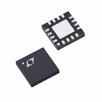
LT5546EUF Linear Technology, LT5546EUF Datasheet

LT5546EUF
Specifications of LT5546EUF
Available stocks
Related parts for LT5546EUF
LT5546EUF Summary of contents
Page 1
... The standby mode provides reduced supply current and fast transient response into the normal operating mode when the I/Q outputs are AC-coupled to a baseband chip. , LTC and LT are registered trademarks of Linear Technology Corporation. All other trademarks are the property of their respective owners. 1.8V ...
Page 2
... CTRL (Note 6) (Note 6) (Note 8) (Note 8) (Notes 6, 8) ≤ 10pF Single Ended, C LOAD (Note –25.5dBm, 280MHz IF –25.5dBm, 280.1MHz (Note 7) IF ORDER PART TOP VIEW NUMBER LT5546EUF 12 STBY + 11 2xLO 17 – 2xLO PART MARKING 5546 UF PACKAGE = 125°C, θ = 37°C –5dBm (Note 5), f ...
Page 3
ELECTRICAL CHARACTERISTICS P = –30dBm, I and Q outputs 800mV IF P-P SYMBOL PARAMETER Variable Gain Amplifier (VGA) Gain Slope Linearity Error Temperature Gain Shift Gain Control Response Time Gain Control Voltage Range Gain Control Slope Gain Control Input Impedance ...
Page 4
LT5546 W U TYPICAL PERFOR A CE CHARACTERISTICS (Note 5 284MHz –30dBm, I and Q outputs 800mV IF IF unless otherwise noted. (Note 3) Supply Current vs Supply Voltage 28 85°C 26 25°C 24 –40°C 22 ...
Page 5
W U TYPICAL PERFOR A CE CHARACTERISTICS (Note 5 284MHz –30dBm, I and Q outputs 800mV IF IF unless otherwise noted. (Note 3) Total Harmonic Distortion vs IF Input Power at 3V Supply and 800mV Differential ...
Page 6
LT5546 W U TYPICAL PERFOR A CE CHARACTERISTICS (Note 5 284MHz –30dBm, I and Q outputs 800mV IF IF unless otherwise noted. (Note 3) IF Detector Output Voltage vs IF Input CW Power and Supply Voltage ...
Page 7
W BLOCK DIAGRA U U APPLICATIO S I FOR ATIO The LT5546 consists of a variable gain amplifier (VGA), I/Q demodulator, quadrature LO generator, lowpass fil- ters (LPFs), clipping amplifiers (clippers) and bias cir- cuitry. The IF signal is fed ...
Page 8
LT5546 U U APPLICATIO S I FOR ATIO C3 L1 56pF 56nH IF INPUT 5.6pF 120nH 56nH Figure 1. Example L-C IF Input Matching Network at 280MHz Table 1. The Component Values of Matching Network L1, L2, ...
Page 9
U U APPLICATIO S I FOR ATIO extended gain control range of –23dB to 57dB. The V pin is a very sensitive input because of its high input impedance and therefore should be well shielded. Signal pickup on the V ...
Page 10
LT5546 U U APPLICATIO S I FOR ATIO then the circuit will limit symmetrically, which will help to prevent the output buffer from overloading. This speeds up recovery from an overload event, which can occur during the gain settling. The ...
Page 11
... Figure 11. 2.4GHz to 2.5GHz Receiver Application ( 280MHz) Information furnished by Linear Technology Corporation is believed to be accurate and reliable. However, no responsibility is assumed for its use. Linear Technology Corporation makes no represen- tation that the interconnection of its circuits as described herein will not infringe on existing patent rights. ...
Page 12
... PIN 1 NOTCH R = 0.20 TYP OR 0.35 × 45° CHAMFER R = 0.115 TYP 15 16 0.55 ± 0. 2.15 ± 0.10 (4-SIDES) (UF16) QFN 10-04 0.30 ± 0.05 0.200 REF 0.00 – 0.05 0.65 BSC LT/LWI/LT 0705 REV A • PRINTED IN USA © LINEAR TECHNOLOGY CORPORATION 2003 5546fa ...


