MW4IC2020GMBR1 Freescale Semiconductor, MW4IC2020GMBR1 Datasheet
MW4IC2020GMBR1
Specifications of MW4IC2020GMBR1


Related parts for MW4IC2020GMBR1

MW4IC2020GMBR1 Summary of contents
Page 1
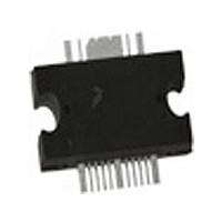
... PLASTIC MW4IC2020MBR1 CASE 1329A - 272 GULL PLASTIC MW4IC2020GMBR1 GND 1 16 GND V 2 DS2 RD1 V 4 RG1 V 5 DS1 V DS3 out GS1 V 9 GS2 GS3 12 GND 11 GND (Top View) Note: Exposed backside flag is source terminal for transistors. Figure 2. Pin Connections MW4IC2020MBR1 MW4IC2020GMBR1 1 ...
Page 2
... Part - to - Part Phase Variation @ out 1. Refer to AN1955, Thermal Measurement Methodology of RF Power Amplifiers http://www.freescale.com/rf. Select Documentation/Application Notes - AN1955. 2. Refer to AN1977, Quiescent Current Thermal Tracking Circuit in the RF Integrated Circuit Family http://www.freescale.com/rf. Select Documentation/Application Notes - AN1977. MW4IC2020MBR1 MW4IC2020GMBR1 2 Stage 1 Stage 2 Stage 3 Rating 3 = 25° ...
Page 3
... Min Typ Max Unit = 80 mA 240 mA 250 mA, DQ1 DQ2 DQ3 — 30 — dB — 5 — % — — dBc — — dBc — — dBc = 26 Vdc mA, DD DQ1 — 29 — dB — 15 — % — 1 — % rms — — dBc — — dBc MW4IC2020MBR1 MW4IC2020GMBR1 3 ...
Page 4
... Microstrip Z4 0.327″ x 0.087″ Microstrip Z5 0.271″ x 0.087″ Microstrip Figure 3. MW4IC2020MBR1(GMBR1) Test Circuit Schematic Table 6. MW4IC2020MBR1(GMBR1) Test Circuit Component Designations and Values Part C1, C2 C5, C6 C9, C11 C10 C12 C13 C14 R1, R2, R3 MW4IC2020MBR1 MW4IC2020GMBR1 4 1 DUT ...
Page 5
... PCBs may have either Motorola or Freescale markings during the transition period. These changes will have no impact on form, fit or function of the current product. Figure 4. MW4IC2020MBR1(GMBR1) Test Circuit Component Layout RF Device Data Freescale Semiconductor MW4IC2020 Rev C11 C12 C10 C14 C13 GND MW4IC2020MBR1 MW4IC2020GMBR1 5 ...
Page 6
... DQ1 DQ2 DQ3 f = 1960 MHz 31 29 η 0 OUTPUT POWER (WATTS) CW out Figure 8. Power Gain and Drain Efficiency versus Output Power MW4IC2020MBR1 MW4IC2020GMBR1 6 TYPICAL CHARACTERISTICS G IRL η Vdc (PEP) out = 80 mA 200 mA 300 mA DQ2 DQ3 IMD 1850 1900 1950 f, FREQUENCY (MHz) − ...
Page 7
... Vdc T = 85_C mA 230 mA 230 mA DQ2 DQ3 25_C −30_C OUTPUT POWER (WATTS) AVG. out = 26 Vdc = 80 mA 230 mA 230 mA DQ2 DQ3 −30_C T = 25_C C 85_C 85_C 25_C −30_C OUTPUT POWER (WATTS) AVG. out versus Output Power @ 1960 MHz MW4IC2020MBR1 MW4IC2020GMBR1 2000 100 100 7 ...
Page 8
... Figure 16. MTTF Factor versus Junction Temperature MW4IC2020MBR1 MW4IC2020GMBR1 8 TYPICAL CHARACTERISTICS 3rd Stage 2nd Stage 1st Stage 90 100 110 120 130 140 150 160 T , JUNCTION TEMPERATURE (°C) J This above graph displays calculated MTTF in hours x ampere drain current. Life tests at elevated temperatures have correlated to better than ± ...
Page 9
... Z = Device input impedance as measured from in gate to ground Test circuit impedance as measured load from drain to ground. Output Device Matching Under Test Network load = 20 W PEP out Ω MW4IC2020MBR1 MW4IC2020GMBR1 9 ...
Page 10
... MW4IC2020MBR1 MW4IC2020GMBR1 10 PACKAGE DIMENSIONS RF Device Data Freescale Semiconductor ...
Page 11
... RF Device Data Freescale Semiconductor MW4IC2020MBR1 MW4IC2020GMBR1 11 ...
Page 12
... MW4IC2020MBR1 MW4IC2020GMBR1 12 RF Device Data Freescale Semiconductor ...
Page 13
... RF Device Data Freescale Semiconductor MW4IC2020MBR1 MW4IC2020GMBR1 13 ...
Page 14
... MW4IC2020MBR1 MW4IC2020GMBR1 14 RF Device Data Freescale Semiconductor ...
Page 15
... RF Device Data Freescale Semiconductor MW4IC2020MBR1 MW4IC2020GMBR1 15 ...
Page 16
... RoHS- compliant and/ free versions of Freescale products have the functionality and electrical characteristics of their non - RoHS- compliant and/or non - Pb- free counterparts. For further information, see http://www.freescale.com or contact your Freescale sales representative. For information on Freescale’s Environmental Products program http://www.freescale.com/epp. MW4IC2020MBR1 MW4IC2020GMBR1 Document Number: MW4IC2020 Rev. 8, 5/2006 16 Information in this document is provided solely to enable system and software implementers to use Freescale Semiconductor products ...