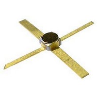
MSA-1120 Avago Technologies US Inc., MSA-1120 Datasheet - Page 2

MSA-1120
Manufacturer Part Number
MSA-1120
Description
AMP MMIC SI BIPOLAR 200-MIL BeO
Manufacturer
Avago Technologies US Inc.
Series
-r
Type
General Purposer
Datasheet
1.MSA-1120.pdf
(4 pages)
Specifications of MSA-1120
Gain
11.5dB ~ 13.5dB
Rf Type
ISM
Current - Supply
40mA ~ 75mA
Frequency
50MHz ~ 1.6GHz
Noise Figure
3.5dB ~ 4.5dB
P1db
16dBm ~ 17.5dBm
Package / Case
4-SMD (100 mil)
Test Frequency
500MHz
Voltage - Supply
4.5V ~ 6.5V
Frequency Range
50MHz To 1.6GHz
Noise Figure Typ
3.5dB
Power Dissipation Pd
650mW
Supply Current
75mA
Supply Voltage Range
4.5V To 6.5V
Number Of Channels
1
Frequency (max)
25GHz
Output Power
17.5@500MHzdBm
Power Supply Requirement
Single
Single Supply Voltage (min)
4.5V
Single Supply Voltage (typ)
5.5V
Single Supply Voltage (max)
6.5V
Package Type
BeO
Dual Supply Voltage (min)
Not RequiredV
Dual Supply Voltage (typ)
Not RequiredV
Dual Supply Voltage (max)
Not RequiredV
Pin Count
4
Mounting
Surface Mount
Lead Free Status / RoHS Status
Lead free / RoHS Compliant
Lead Free Status / RoHS Status
Lead free / RoHS Compliant, Lead free / RoHS Compliant
Available stocks
Company
Part Number
Manufacturer
Quantity
Price
Part Number:
MSA-1120
Manufacturer:
AVAGO/安华高
Quantity:
20 000
Company:
Part Number:
MSA-1120-BLK
Manufacturer:
AVAGO
Quantity:
1 020
Company:
Part Number:
MSA-1120-TR1
Manufacturer:
AMS
Quantity:
301
Electrical Specifications
MSA-1120 Absolute Maximum Ratings
Notes:
1. Permanent damage may occur if any of these limits are exceeded.
2. T
3. Derate at 16.7 mW/°C for T
4. The small spot size of this technique results in a higher, though more accurate determination
Notes:
1. The recommended operating current range for this device is 40 to 75 mA.
2. Referenced from 50 MHz gain (GP).
Parameter
Device Current
Power Dissipation
RF Input Power
Junction Temperature
Storage Temperature
Symbol
VSWR
G
∆G
f
NF
P
IP
t
V
dV/dT
3 dB
D
1 dB
d
P
3
of θ
Typical performance as a function of current is on the following page.
CASE
P
jc
than do alternate methods.
= 25°C.
[,3]
Parameters and Test Conditions: I
Power Gain (|S
Gain Flatness
3 dB Bandwidth
Input VSWR
Output VSWR
50 Ω Noise Figure
Output Power at 1 dB Gain Compression
Third Order Intercept Point
Group Delay
Device Voltage
Device Voltage Temperature Coefficient
[1]
C
> 161°C.
, T
1
A
[]
|
= 25°C
)
d
= 60 mA, Z
Absolute Maximum
–65 to 00°C
+13 dBm
650 mW
100 mA
f = 0.1 GHz
f = 0.1 to 1.0 GHz
f = 0.1 to 1.5 GHz
f = 0.1 to 1.5 GHz
f = 0.5 GHz
f = 0.5 GHz
f = 0.5 GHz
f = 0.5 GHz
O
00°C
= 50 Ω
[1]
Thermal Resistance
θ
jc
= 60°C/W
Units
mV/°C
dBm
dBm
psec
GHz
dB
dB
dB
V
Min.
11.5
16.0
[2,4]
4.5
:
Typ.
±0.7
1.7:1
1.9:1
–8.0
1.5
17.5
30.0
00
1.6
3.5
5.5
Max.
±1.0
13.5
4.5
6.5


