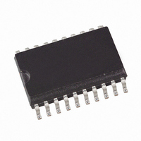
ATR4251-TKSY Atmel, ATR4251-TKSY Datasheet - Page 9

ATR4251-TKSY
Manufacturer Part Number
ATR4251-TKSY
Description
IC ANTENNA AMP AM/FM LN 20SSOP
Manufacturer
Atmel
Specifications of ATR4251-TKSY
Current - Supply
14mA
Frequency
150kHz ~ 30MHz, 70MHz ~ 110MHz
Gain
6dB
Package / Case
20-SOIC (0.200", 5.30mm Width)
Rf Type
Broadcast Radio
Voltage - Supply
8 V ~ 11 V
Operating Temperature (min)
-40C
Operating Temperature Classification
Industrial
Mounting
Surface Mount
Pin Count
20
Lead Free Status / RoHS Status
Lead free / RoHS Compliant
Noise Figure
-
P1db
-
Test Frequency
-
Lead Free Status / Rohs Status
Compliant
7. Electrical Characteristics (Continued)
See Test Circuit,
package.
4913J–AUDR–10/09
Parameters Dependent of External Components in Application Circuit: R
*) Type means: A = 100% tested, B = 100% correlation tested, C = Characterized on samples, D = Design parameter
Notes:
3.10
3.11
3.12
4.10
4.11
4.12
No.
3.9
4.1
4.2
4.3
4.4
4.5
4.6
4.7
4.8
4.9
5.1
5.2
5.3
5.4
5.5
5.6
4
5
1. Leakage current of PIN diode can be adjusted by an external resistor between pin 11 and VS
2. Demo board measurements (see
3. Demo board measurements (see
Parameters
Transconductance of
Level detector
IP3 at level detector
input
PIN diode current
generation
Output resistance
FM Amplifier
Emitter voltage
Emitter voltage
Supply current limit
Maximum output
voltage
Input resistance
Output resistance
Power gain
Output noise voltage
(emitter circuit)
OIP3 (emitter circuit)
Gain
Noise figure
OIP3
FM AGC
AGC threshold
AGC1 output voltage
AGC1 output voltage
AGC2 output voltage
AGC2 output voltage
Input resistance
(3)
(3)
Figure 8-1 on page
(2)
(3)
(2)
(2)
Test Conditions
ViHF = V
Figure 9-2 on page
1 MHz and 1,1MHz,
120 dBµV
d(20 log I
T = 25°C, U
T = –40°C to +85°C
R = 56
V
f = 100 MHz
f = 100 MHz
f = 100 MHz
f = 100 MHz,
B = 120 kHz
f = 98 + 99 MHz
f = 98 + 99 MHz
f = 100 MHz
f = 900 MHz
AGC1 active,
V
AGC1 inactive,
V
AGC2 active,
V
AGC2 inactive,
V
S
pin16 (16)
pin16 (16)
pin16
pin16
11; V
= 10V
(16) = 1.7V
(16) = 5V
S
AMth
= 10V, T
Pin-diode
= 5V
= 1.7V
Pin12
Figure 8-1 on page 11
Figure 9-1 on page 12
at pin 10 (9)
) / dU
= 2V
amb
13,
= 25°C, unless otherwise specified. Pin numbers in () are referred to the QFN
Pin12
FMOUT/
19 (20)
19 (20)
19 (20)
19 (20)
19 (20)
18 (19)
18 (19)
(9/11)
10 (9)
1 (22)
1 (22)
2 (23)
5 (24)
5 (24)
10/12
FMIN
9 (8)
6 (4)
6 (4)
Pin
“Common Emitter Configuration”)
“Common Base Configuration”)
Symbol
I
-------------------
R
V
AM sin k
V
V
R
R
R
V
V
V
V
FMOUT
th1,100
I
thl,900
AMth
I
V
Pin18
FMIN
AGC
AGC
AGC
AGC
OUT
G
IP3
19
N
FMIN
, R
FMOUT
V
V
V
V
S
S
S
S
Min.
1.85
150
1.8
– 2.1V V
– 0.2V
– 2.1V V
– 0.2V
27
12
81
81
17
, G, V
N
, IIP3
S
S
Typ.
1.95
–5.1
170
140
148
2.0
2.8
– 1.9V V
– 1.9V V
20
30
35
50
50
83
85
V
V
21
5
6
S
S
S
S
Max.
2.05
– 1.7V
– 1.7V
2.2
45
37
85
87
25
ATR4251
---------------- -
mV
dBµV
dBµV
dBµV
dBµV
dBµV
dBµV
dB/V
Unit
mA
V
µA
dB
dB
dB
k
k
V
V
V
V
V
V
pp
rms
Type*
C
D
D
D
A
C
D
D
D
D
A
D
C
C
C
C
B
B
C
C
C
C
D
9


