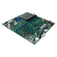
M52277EVB Freescale Semiconductor, M52277EVB Datasheet - Page 24
M52277EVB
Manufacturer Part Number
M52277EVB
Description
BOARD DEMO FOR MCF5227
Manufacturer
Freescale Semiconductor
Series
ColdFire®r
Type
MCUr
Specifications of M52277EVB
Contents
Board
Silicon Manufacturer
Freescale
Core Architecture
Coldfire
Core Sub-architecture
Coldfire V2
Silicon Core Number
MCF52
Silicon Family Name
MCF5227x
Peak Reflow Compatible (260 C)
Yes
Rohs Compliant
Yes
For Use With/related Products
MCF52277
Lead Free Status / RoHS Status
Lead free / RoHS Compliant


1
2
3
4
5
6
7
Electrical Characteristics
24
SD10 Data Input Hold relative to SD_CLK (reference only)
SD11 Data (D[31:0]) and Data Mask(SD_DQM[3:0]) Output Valid
SD12 Data (D[31:0]) and Data Mask (SD_DQM[3:0]) Output Hold
Num
SD8 SD_DQS[3:2] input hold relative to SD_CLK
SD9 Data (D[31:0]) Input Setup relative to SD_CLK (reference
The device supports same frequency of operation for both FlexBus and SDRAM clock operates as that of the internal bus clock.
Please see the PLL chapter of the device reference manual for more information on setting the SDRAM clock rate.
SD_CLK is one SDRAM clock in ns.
Pulse width high plus pulse width low cannot exceed min and max clock period.
SD_SDR_DQS is designed to pulse 0.25 clock before the rising edge of the memory clock. This is a guideline only. Subtle
variation from this guideline is expected. SD_SDR_DQS will only pulse during a read cycle and one pulse will occur for each
data beat.
SD_DQS is designed to pulse 0.25 clock before the rising edge of the memory clock. This spec is a guideline only. Subtle
variation from this guideline is expected. SD_DQS will only pulse during a read cycle and one pulse will occur for each data
beat.
The SD_DQS pulse is designed to be 0.5 clock in width. The timing of the rising edge is most important. The falling edge does
not affect the memory controller.
Since a read cycle in SDR mode still uses the DQS circuit within the device, it is critical that the data valid window be centered
1/4 clk after the rising edge of DQS. Ensuring that this happens will result in successful SDR reads. The input setup spec is
provided as guidance.
SD_BA[1:0]
only)
SD_RAS
SD_CAS
SD_CSn
SD_CLK
SD_WE
A[23:0]
D[31:0]
SDDM
SD4
Characteristic
ROW
CMD
MCF5227x ColdFire
Table 14. SDR Timing Specifications (continued)
SD1
SD5
Figure 11. SDR Write Timing
WD1
COL
®
Microprocessor Data Sheet, Rev. 8
SD11
SD12
WD2
t
t
t
SDCHDMV
Symbol
t
DQISDCH
SDCHDMI
t
DVSDCH
DISDCH
WD3
SD2
SD_CLK
Does not apply. 0.5×SD_CLK fixed
0.25 ×
Min
1.0
1.5
—
WD4
0.5 × SD_CLK
width.
Max
+ 2
—
—
—
Freescale Semiconductor
SD3
Unit
ns
ns
ns
ns
Notes
6
7
Related parts for M52277EVB
Image
Part Number
Description
Manufacturer
Datasheet
Request
R

Part Number:
Description:
Manufacturer:
Freescale Semiconductor, Inc
Datasheet:
Part Number:
Description:
Manufacturer:
Freescale Semiconductor, Inc
Datasheet:
Part Number:
Description:
Manufacturer:
Freescale Semiconductor, Inc
Datasheet:
Part Number:
Description:
Manufacturer:
Freescale Semiconductor, Inc
Datasheet:
Part Number:
Description:
Manufacturer:
Freescale Semiconductor, Inc
Datasheet:
Part Number:
Description:
Manufacturer:
Freescale Semiconductor, Inc
Datasheet:
Part Number:
Description:
Manufacturer:
Freescale Semiconductor, Inc
Datasheet:
Part Number:
Description:
Manufacturer:
Freescale Semiconductor, Inc
Datasheet:
Part Number:
Description:
Manufacturer:
Freescale Semiconductor, Inc
Datasheet:
Part Number:
Description:
Manufacturer:
Freescale Semiconductor, Inc
Datasheet:
Part Number:
Description:
Manufacturer:
Freescale Semiconductor, Inc
Datasheet:
Part Number:
Description:
Manufacturer:
Freescale Semiconductor, Inc
Datasheet:
Part Number:
Description:
Manufacturer:
Freescale Semiconductor, Inc
Datasheet:
Part Number:
Description:
Manufacturer:
Freescale Semiconductor, Inc
Datasheet:
Part Number:
Description:
Manufacturer:
Freescale Semiconductor, Inc
Datasheet: