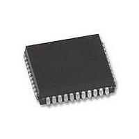
XR88C681J-F Exar Corporation, XR88C681J-F Datasheet - Page 62

XR88C681J-F
Manufacturer Part Number
XR88C681J-F
Description
IC UART CMOS DUAL 44PLCC
Manufacturer
Exar Corporation
Type
CMOS Dual Channel UARTr
Datasheet
1.XR88C681CP40-F.pdf
(101 pages)
Specifications of XR88C681J-F
Number Of Channels
2, DUART
Package / Case
44-LCC (J-Lead)
Features
*
Fifo's
1 Byte, 3 Byte
Voltage - Supply
5V
With Parallel Port
Yes
With Cmos
Yes
Mounting Type
Surface Mount
Data Rate
1 Mbps
Supply Voltage (max)
5.25 V
Supply Voltage (min)
4.75 V
Supply Current
15 mA
Maximum Operating Temperature
+ 85 C
Minimum Operating Temperature
- 40 C
Mounting Style
SMD/SMT
Operating Supply Voltage
5 V
Propagation Delay Time Ns
400 ns
No. Of Channels
2
Supply Voltage Range
4.75V To 5.25V
Operating Temperature Range
-40°C To +85°C
Digital Ic Case Style
PLCC
No. Of Pins
44
Filter Terminals
SMD
Rohs Compliant
Yes
Lead Free Status / RoHS Status
Lead free / RoHS Compliant
Lead Free Status / RoHS Status
Lead free / RoHS Compliant, Lead free / RoHS Compliant
Other names
1016-1329
Available stocks
Company
Part Number
Manufacturer
Quantity
Price
Company:
Part Number:
XR88C681J-F
Manufacturer:
Exar Corporation
Quantity:
10 000
This spec is not related to the parameter tRTX, which also
specifies limits on signals applied to IP2 or other input
pins, for use at the External Clock Source for Transmitter
and Receivers.
D t
This spec places a lower limit on the amount of time that a
signal, being applied at the General Purpose Input Pins,
IP2 - IP5, for use as the Transmitter and Receiver Clock
source, can reside at the high or low state. This spec has
no relationship to t
Input pin IP2.
D f
This spec places limits on both the 1X and 16X external
signals that are to be used to clock the Transmitters and
Receivers. If the user wishes to use a 1X clock, he/she
can only apply a signal with frequencies up to 1.0 MHz.
This input will results in a bit rate of 1 Mbps (see Example
C). If the user wishes to use a 16X clock, he/she can only
apply a signal with frequencies up to 2.0 MHz. Since this
signal is a 16X signal, this will result in a bit rate of
125kbps.
In summary, the DUART Timing Control block gives the
user the ability to generate virtually any baud rate that he
- via IP2, IP3, IP4 and IP5
IP2, IP3, IP4, and IP5
RTX
RTX
Rev. 2.11
- RXC and TXC (External) High or Low Time
- RXC and TXC (External) Frequency - via
CTC
, even though it is also applies to
62
or she desires. The Timing Control Block gives the user
access to the following resources:
D 23 different standard bit rates via the BRG.
D The Counter/Timer, which can be configured to gen-
D Inputs to the Timing Control Block (via some Input
E. INPUT PORT
The Input Port can be used as a general purpose input or
the DUART can be programmed to use some of these
inputs for special functions. The current state of the
inputs to this unlatched port can be read by the CPU by
reading the IP register (for the states of IP0 - IP5). A high
input signal at the IPn pin results in a logic “1” in the IPR[n]
bit position, within the IP register. Likewise, a “low” input
signal at the IPn pin results in a logic “0” in the IPR[n] bit
position, within the IP register.
E.1 Alternate Functions for the Input Port
Table 17 describes the alternate uses for the input pins,
such as clock inputs and data flow control signals and
includes a brief summary as how to program the alternate
function. A read of the IP registers will show the logic state
at the pin, regardless of its programmed function.
erate bit rates which are not available from the BRG.
Port pins) which allows the use of external clock sig-
nals to generate a custom bit rate.


