MIC5212-SJBM Micrel Inc, MIC5212-SJBM Datasheet - Page 3
MIC5212-SJBM
Manufacturer Part Number
MIC5212-SJBM
Description
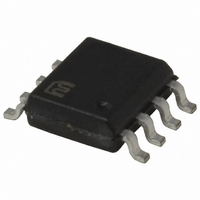
IC REG LDO DUAL 500MA 1% 8-SOIC
Manufacturer
Micrel Inc
Datasheet
1.MIC5212-SJYM.pdf
(9 pages)
Specifications of MIC5212-SJBM
Regulator Topology
Positive Fixed
Voltage - Output
3.3V, 2.5V
Voltage - Input
2.5 ~ 16 V
Voltage - Dropout (typical)
0.35V @ 500mA
Number Of Regulators
2
Current - Output
500mA
Operating Temperature
-40°C ~ 125°C
Mounting Type
Surface Mount
Package / Case
8-SOIC (3.9mm Width)
Lead Free Status / RoHS Status
Contains lead / RoHS non-compliant
Current - Limit (min)
-
Available stocks
Company
Part Number
Manufacturer
Quantity
Price

Part Number:
MIC5212-SJBM
Manufacturer:
MICREL/麦瑞
Quantity:
20 000


Absolute Maximum Ratings
Supply Input Voltage (V
Power Dissipation (P
Storage Temperature Range ................... –60 C to +150 C
Lead Temperature (soldering, 5 sec.) ....................... 260 C
Electrical Characteristics
Regulator A and B V
Symbol
V
V
I
PSRR
I
Note 1.
Note 2.
Note 3.
Note 4.
Note 5.
Note 6.
Note 7.
April 2003
MIC5212
GND
LIMIT
V
V
V
O
IN
O
O
O
– V
/ T
/V
/V
O
O
O
Exceeding the absolute maximum rating may damage the device.
The device is not guaranteed to function outside its operating rating.
Absolute maximum ratings indicate limits beyond which damage to the component may occur. Electrical specifications do not apply when
operating the device outside of its operating ratings. The maximum allowable power dissipation is a function of the maximum junction
temperature, T
dissipation at any ambient temperature is calculated using: P
tion will result in excessive die temperature, and the regulator will go into thermal shutdown. The
mounted on a PC board (see
Output voltage temperature coefficient is defined as the worst case voltage change divided by the total temperature range.
Regulation is measured at constant junction temperature using low duty cycle pulse testing. Parts are tested for load regulation in the load
range from 0.1mA to 500mA. Changes in output voltage due to heating effects are covered by the thermal regulation specification.
Dropout voltage is defined as the input to output differential at which the output voltage drops 2% below its nominal value measured at 1V
differential.
Ground pin current is the regulator quiescent current plus pass transistor base current. The total current drawn from the supply is the sum of
the load current plus the ground pin current.
Parameter
Output Voltage Accuracy
Output Voltage
Temperature Coefficient
Line Regulation
Load Regulation
Dropout Voltage, Note 6
(per regulator)
Ground Pin Current, Note 7
(per regulator)
Ripple Rejection
Current Limit
Spectral Noise Density
J(max)
IN
D
) ............................ Internally Limited
= V
IN
, the junction-to-ambient thermal resistance,
OUT
A or B) ................. –20V to +20V
+ 1V; I
“Thermal Considerations”
L
= 100 A; C
(Note 1)
L
= 4.7 F; T
Conditions
variation from specified V
Note 4
V
I
I
I
I
I
f = 120Hz, I
V
V
L
L
L
L
L
IN
OUT
OUT
= 0.1mA to 500mA, Note 5
= 150mA
= 500mA
= 150mA
= 500mA
= V
section for further details).
= 0V
= 2.5V, I
OUT
D(max)
J
L
= 25 C, bold values indicate –40 C
+ 1V to 16V
3
= 150mA
JA
OUT
= (T
, and the ambient temperature, T
Operating Ratings
Supply Input Voltage (V
Junction Temperature (T
Thermal Resistance
J(max)
= 50mA, C
– T
OUT
A
)
OUT
JA
. Exceeding the maximum allowable power dissipa-
= 2.2 F
JA
JA
IN
J
)......................................... Note 3
) ............................... 2.5V to 16V
of the 8-lead SOIC (M) is 63 C/W
) ....................... –40 C to +125 C
A
(Note 2)
. The maximum allowable power
Min
–1
–2
T
J
+125 C; unless noted.
Typical
0.009
0.05
175
350
750
500
1.5
40
12
75
1000
Max
0.05
275
350
500
600
0.1
0.7
1.0
2.5
3.0
20
25
1
2
MIC5212
ppm/ C
nV/ Hz
Micrel
Units
% / V
% / V
dB5
mV
mV
mV
mV
mA
mA
mA
mA
mA
%
%
%
%
Related parts for MIC5212-SJBM
Image
Part Number
Description
Manufacturer
Datasheet
Request
R

Part Number:
Description:
500mA 1% Low Noise LDO( )
Manufacturer:
Micrel Inc
Datasheet:

Part Number:
Description:
IC REG LDO DUAL 500MA 1% 8-SOIC
Manufacturer:
Micrel Inc
Datasheet:
Part Number:
Description:
500mA 1% Low Noise LDO( )
Manufacturer:
Micrel Inc
Datasheet:
Part Number:
Description:
Manufacturer:
Micrel Inc
Datasheet:
Part Number:
Description:
Manufacturer:
Micrel Inc
Datasheet:
Part Number:
Description:
Manufacturer:
Micrel Inc
Datasheet:
Part Number:
Description:
Manufacturer:
Micrel Inc
Datasheet:
Part Number:
Description:
Manufacturer:
Micrel Inc
Datasheet:
Part Number:
Description:
Manufacturer:
Micrel Inc
Datasheet:
Part Number:
Description:
Manufacturer:
Micrel Inc
Datasheet:
Part Number:
Description:
Manufacturer:
Micrel Inc
Datasheet:
Part Number:
Description:
Manufacturer:
Micrel Inc
Datasheet:
Part Number:
Description:
Manufacturer:
Micrel Inc
Datasheet:
Part Number:
Description:
Manufacturer:
Micrel Inc
Datasheet: