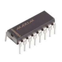
MAX791EPE+ Maxim Integrated Products, MAX791EPE+ Datasheet - Page 8

MAX791EPE+
Manufacturer Part Number
MAX791EPE+
Description
IC SUPERVISOR MPU 16-DIP
Manufacturer
Maxim Integrated Products
Type
Battery Backup Circuitr
Datasheet
1.MAX791CSE.pdf
(19 pages)
Specifications of MAX791EPE+
Number Of Voltages Monitored
1
Output
Push-Pull, Totem Pole
Reset
Active Low
Reset Timeout
140 ms Minimum
Voltage - Threshold
4.65V
Operating Temperature
-40°C ~ 85°C
Mounting Type
Through Hole
Package / Case
16-DIP (0.300", 7.62mm)
Monitored Voltage
4.65 V
Undervoltage Threshold
4.5 V
Overvoltage Threshold
4.75 V
Output Type
Active Low, Open Drain, Push-Pull
Manual Reset
Resettable
Watchdog
Watchdog
Battery Backup Switching
Backup
Power-up Reset Delay (typ)
280 ms
Supply Voltage (max)
5.5 V
Supply Voltage (min)
0 V
Supply Current (typ)
150 uA
Maximum Power Dissipation
842 mW
Maximum Operating Temperature
+ 85 C
Mounting Style
Through Hole
Minimum Operating Temperature
- 40 C
Power Fail Detection
Yes
Lead Free Status / RoHS Status
Lead free / RoHS Compliant
Microprocessor Supervisory Circuit
Figure 1. MAX791 Block Diagram
Many µP-based products require manual-reset capabil-
ity, allowing the operator or test technician to initiate a
reset. The Manual Reset Input (MR) can be connected
directly to a switch, without an external pull-up resistor
or debouncing network. It connects to a 1.25V com-
parator, and has a pull-up to V
1. The propagation delay from asserting MR to RESET
asserted is 4µs typ. Pulsing MR low for a minimum of
15µs resets all the internal counters, sets the Watchdog
Output (WDO) and Watchdog-Pulse Output (WDPO)
8
SWT
V
WDI
_______________Detailed Description
MR
PFI
CC
VBATT
CE IN
_______________________________________________________________________________________
13
11
3
1
9
8
7
V
OUT
4.65V
1.25V
4
150mV
TIMEBASE FOR
CHIP-ENABLE
GENERATION
GND
WATCHDOG
WATCHDOG
TRANSITION
RESET AND
CONTROL
DETECTOR
OUTPUT
RESET
Manual Reset Input
OUT
MAX791
as shown in Figure
WATCHDOG
TIMER
10
LOWLINE
BATT ON
12
15
16
14
5
2
6
CE OUT
V
RESET
WDPO
WDO
PFO
OUT
high, and sets the Set Watchdog-Timeout (SWT) input
to V
(for internal timeouts). It also disables the chip-enable
function, setting the Chip-Enable Output (CE OUT) to a
high state. The RESET output remains active as long as
MR is held low, and the reset-timeout period begins
after MR returns high (Figure 2).
Use this input as either a digital-logic input or a second
low-line comparator. Normal TTL/CMOS levels can be
wire-OR connected via pull-down diodes (Figure 3),
and open-drain/collector outputs can be wire-ORed
directly.
Figure 2. Manual-Reset Timing Diagram
Figure 3. Diode "OR" Connections Allow Multiple Reset Sources
to Connect to MR
SOURCES
OUT
OTHER
CE OUT
RESET
RESET
CE IN
* DIODES NOT REQUIRED ON OPEN-DRAIN OUTPUTS
MR
0V
MANUAL RESET
- 0.6V, if it is not already connected to V
*
*
MR
25µs MIN
MAX791
7.5µs TYP
15µs TYP
OUT


