5962-8773802GA Analog Devices Inc, 5962-8773802GA Datasheet - Page 11
5962-8773802GA
Manufacturer Part Number
5962-8773802GA
Description
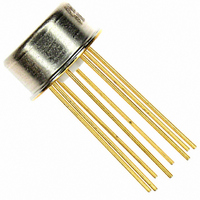
IC OPAMP GP 600KHZ LP TO99-8
Manufacturer
Analog Devices Inc
Datasheet
1.5962-8773802GA.pdf
(16 pages)
Specifications of 5962-8773802GA
Slew Rate
0.3 V/µs
Amplifier Type
General Purpose
Number Of Circuits
1
Gain Bandwidth Product
600kHz
Current - Input Bias
2.4nA
Voltage - Input Offset
25µV
Voltage - Supply, Single/dual (±)
±3 V ~ 18 V
Operating Temperature
-55°C ~ 125°C
Mounting Type
Through Hole
Package / Case
TO-99-8, Metal Can
Rail/rail I/o Type
No
Number Of Elements
1
Common Mode Rejection Ratio
120dB
Input Offset Voltage
0.025@±15VmV
Single Supply Voltage (typ)
Not RequiredV
Dual Supply Voltage (typ)
±5/±9/±12/±15V
Voltage Gain In Db
133.98dB
Power Supply Rejection Ratio
110.46dB
Power Supply Requirement
Dual
Shut Down Feature
No
Single Supply Voltage (min)
Not RequiredV
Single Supply Voltage (max)
Not RequiredV
Dual Supply Voltage (min)
±3V
Dual Supply Voltage (max)
±22V
Technology
Bipolar
Operating Temp Range
-55C to 125C
Operating Temperature Classification
Military
Mounting
Through Hole
Pin Count
8
Package Type
TO-99
Lead Free Status / RoHS Status
Lead free / RoHS Compliant
Current - Supply
-
Output Type
-
Current - Output / Channel
-
-3db Bandwidth
-
Lead Free Status / RoHS Status
Not Compliant, Lead free / RoHS Compliant
Other names
Q3964209
Available stocks
Company
Part Number
Manufacturer
Quantity
Price


APPLICATIONS
The high gain, gain linearity, CMRR, and low TCV
OP77 make it possible to obtain performance not previously
available in single-stage, very high-gain amplifier applications.
For best CMR,
10 mV differential signal, the maximum errors are as listed in
Table 7.
Table 7. Maximum Errors
Type
Common-Mode Voltage
Gain Linearity, Worst Case
TCV
TCI
This circuit reduces maximum slew rate but allows driving
capacitive loads of any size without instability. Because the boon
resistor is inside the feedback loop, its effect on output
impedance is reduced to insignificance by the high open-loop
gain of the OP77.
OS
OS
INPUT
Figure 27. Precision High-Gain Differential Amplifier
V
IN
Figure 28. Isolating Large Capacitive Loads
R
100kΩ
100kΩ
R
R
S
R1
R2
1
2
1kΩ
1kΩ
Figure 29. Basic Current Source
R1
R3
must equal
10µF
2
3
2
3
OP77
+15V
–15V
OP77
R4
1MΩ
2
3
4
7
0.1µF
0.1µF
OP77E
990Ω
R
1kΩ
R3
R4
+15V
–15V
F
1MΩ
6
R2
7
4
R
R
0.1µF
0.1µF
6
3
4
. In this example, with a
6
100Ω
R5
10Ω
I
OUT
Amount
0.01%/V
0.02%
0.003%/°C
0.008%/°C
< 15mA
C
LOAD
OUTPUT
OS
of the
Rev. E | Page 11 of 16
These current sources can supply both positive and negative
current into a grounded load.
Note that
And that for Z
V
IN
Z
O
=
R1
R2
R
R
5
5
R
⎛
⎜
⎝
O
+
2
3
2
R
R
to be infinite
R
4
2
OP77
Figure 30. 100 mA Current Source
4
I
GIVEN R3 = R4 + R5, R1 = R2
OUT
+
R
R
1
3
1
⎞
⎟
⎠
= V
IN
6
(
R3
R4
R1 – R5
R3
R +
5
R
)
2
+15V
–15V
R
2N2222
2N2907
4
must =
R5
I
OUT
R
R
3
1
< 100mA
OP77
Related parts for 5962-8773802GA
Image
Part Number
Description
Manufacturer
Datasheet
Request
R

Part Number:
Description:
OPTOCOUPLER HERMETIC 8-DIP
Manufacturer:
Avago Technologies US Inc.
Datasheet:

Part Number:
Description:
OPTOCOUPLER HERMETIC 8-DIP GW
Manufacturer:
Avago Technologies US Inc.
Datasheet:

Part Number:
Description:
Analog Multiplexer Single 8:1 16-Pin CDIP
Manufacturer:
Intersil
Datasheet:

Part Number:
Description:
ADC Single Semiflash 400KSPS 8-Bit Parallel 24-Pin CDIP
Manufacturer:
Maxim Integrated Products
Datasheet:
Part Number:
Description:
Analog Multiplexer Single 8:1 16-Pin CDIP
Manufacturer:
Maxim Integrated Products
Datasheet:
Part Number:
Description:
Analog Multiplexer Dual 8:1 28-Pin CDIP
Manufacturer:
Intersil
Datasheet:
Part Number:
Description:
CDIP 8/M�/Precision CMOS Analog Switch
Manufacturer:
Maxim Integrated Products

Part Number:
Description:
SPLD, PALCE16V8 Family, EECMOS Process, 300 Gates, 8 Macro Cells, 8 Reg., 8 User I/Os, 5V Supply, 15 Speed Grade, 20DIP
Manufacturer:
Cypress Semiconductor Corporation.
Datasheet:
Part Number:
Description:
OPTOCOUPLER MOSFET HERM 8DIP
Manufacturer:
Avago Technologies US Inc.
Datasheet:
Part Number:
Description:
OPTOCOUPLER GATE HERM SEAL 8DIP
Manufacturer:
Avago Technologies US Inc.
Datasheet:
Part Number:
Description:
OPTOCOUPLER GATE HERM SEAL 8DIP
Manufacturer:
Avago Technologies US Inc.
Datasheet:
Part Number:
Description:
OPTOCOUPLER GATE HERM SEAL 8DIP
Manufacturer:
Avago Technologies US Inc.
Datasheet:

Part Number:
Description:
ADC, LC2MOS High Speed 4-and 8-Channel 8-Bit ADCs
Manufacturer:
Analog Devices
Part Number:
Description:
ADC, LC2MOS High Speed 4-and 8-Channel 8-Bit ADCs
Manufacturer:
Analog Devices
Part Number:
Description:
OPTOCOUPLER HIGH CMR HERM 8DIP
Manufacturer:
Avago Technologies US Inc.
Datasheet: