MCP655-E/UN Microchip Technology, MCP655-E/UN Datasheet
MCP655-E/UN
Specifications of MCP655-E/UN
Available stocks


Related parts for MCP655-E/UN


MCP655-E/UN Summary of contents
Page 1
... This family is offered in single with CAL/CS pin (MCP651), dual (MCP652) and dual with CAL/CS pins (MCP655). All devices are fully specified from -40°C to +125°C. Typical Application Circuit R 1 ...
Page 2
... MCP651/2/5 NOTES: DS22146A-page 2 © 2009 Microchip Technology Inc. ...
Page 3
... The I specifications are for design guidance only; they are not tested. SC © 2009 Microchip Technology Inc. † Notice: Stresses above those listed under “Absolute Maximum Ratings” may cause permanent damage to the device. This is a stress rating only and functional operation of ...
Page 4
... V/µs E — 17 — µ — 7.5 — nV/√ MHz — fA/√ GND / Units Conditions mV V pin externally driven CAL V pin open CAL kΩ|| GND / 1-2). Conditions ° Ω + kHz, OUT P 5.5V kHz + 100 mV OUT kHz © 2009 Microchip Technology Inc. ...
Page 5
... This time ensures that the internal logic recognizes the edge. However, for the rising edge case, if CAL/CS is raised before the calibration is complete, the calibration will be aborted and the part will return to low power mode. 3: For the MCP655 dual, there is an additional constraint. CAL (within a time much smaller than t gled independently, then CAL A calibration mode ...
Page 6
... V IN– (V/V) 10 kΩ (V) (mV) FIGURE 1-2: Most Specifications. = +2.5V to +5.5V GND. SS Conditions IL V PRL t t CON POFF High (typical) -3 µA (typical (typical 6 kΩ 100 nF 2.2 µF V OUT kΩ kΩ 6 and DC Test Circuit for © 2009 Microchip Technology Inc. ...
Page 7
... Calibration Calibration 15% Changed Changed 10 -100 -80 -60 -40 - Input Offset Voltage Repeatability (µV) FIGURE 2-3: Input Offset Voltage Repeatability (repeated calibration). © 2009 Microchip Technology Inc. = +2.5V to 5.5V GND 700 600 500 400 300 200 100 0 -100 60 80 100 1.5 2.0 2.5 3.0 3.5 4.0 4.5 5.0 5.5 6.0 6.5 FIGURE 2-4: Power Supply Voltage ...
Page 8
... Currents vs. Ambient Temperature with V = +5. OUT DD PSRR CMRR 5.5V DD CMRR 2. 100 125 Ambient Temperature (°C) CMRR and PSRR vs 5. 2. 100 125 Ambient Temperature (°C) DC Open-Loop Gain vs 5. CMR_H 105 125 Ambient Temperature (°C) Input Bias and Offset © 2009 Microchip Technology Inc. ...
Page 9
... Common Mode Input Voltage (V) FIGURE 2-14: Input Bias and Offset Currents vs. Common Mode Input Voltage with T = +125°C. A © 2009 Microchip Technology Inc. = +2.5V to 5.5V GND 1.E- ...
Page 10
... FIGURE 2-21: vs. Ambient Temperature / / OUT DD +125°C +85°C +25°C -40°C Power Supply Voltage (V) Supply Current vs. Power 2.5V DD Common Mode Input Voltage (V) Supply Current vs. Common V PRH V PRL 100 125 Ambient Temperature (°C) Power On Reset Voltages © 2009 Microchip Technology Inc. ...
Page 11
... pF, and CAL/ 30% 144 Samples 25 2.5V and 5.5V DD 20% 15% 10 Normalized Internal Calibration Voltage CAL DD FIGURE 2-22: Normalized Internal Calibration Voltage. © 2009 Microchip Technology Inc. = +2.5V to 5.5V GND 140 120 100 -50 -25 0 Ambient Temperature (°C) FIGURE 2-23: V Temperature. MCP651/2/5 / ...
Page 12
... FIGURE 2-29: Impedance vs. Frequency / / OUT 5. 2. GBWP 20 10 Common Mode Input Voltage (V) Gain Bandwidth Product 5. GBWP 2. Output Voltage (V) Gain Bandwidth Product V/V 10k 100k 1M 10M 100M Frequency (Hz) Closed-Loop Output © 2009 Microchip Technology Inc. ...
Page 13
... CAL • 10p 100p 1n 1.0E-11 1.0E-10 Normalized Capacitive Load; C FIGURE 2-30: Gain Peaking vs. Normalized Capacitive Load. © 2009 Microchip Technology Inc. = +2.5V to 5.5V GND 150 140 130 120 110 100 10n 1k 1.0E-09 1.E+03 /G (F) L FIGURE 2-31: Separation vs. Frequency. MCP651/2 ...
Page 14
... FIGURE 2-35: Time with 0.1 Hz Filter > 500 kHz 0.01 0.001 kHz 0.0001 100 1.E+2 FIGURE 2-36: = GND / OUT Time (min) Input Noise plus Offset V/V 1k 10k 100k 1.E+3 1.E+4 1.E+5 Frequency (Hz) THD+N vs. Frequency. © 2009 Microchip Technology Inc. /2, ...
Page 15
... Non-inverting Large Signal Step Response 5. 499Ω OUT 0 50 100 150 200 250 300 Time (ns) FIGURE 2-39: Inverting Small Signal Step Response. © 2009 Microchip Technology Inc. = +2.5V to 5.5V GND 5 5. 4.5 4.0 3.5 3.0 2.5 2.0 1.5 1.0 0.5 0.0 0 ...
Page 16
... MCP651/2/5 Note: Unless otherwise indicated +25° / kΩ pF, and CAL 0.1 100k 1M 10M 1.E+05 1.E+06 1.E+07 Frequency (Hz) FIGURE 2-43: Maximum Output Voltage Swing vs. Frequency. DS22146A-page 16 = +2.5V to 5.5V GND 100M 1.E+ / /2, DD OUT DD © 2009 Microchip Technology Inc. ...
Page 17
... CAL/ OUT Time (ms) FIGURE 2-46: CAL/CS Voltage, Output Voltage and Supply Current (for Side A) vs. Time with V = 5.5V. DD © 2009 Microchip Technology Inc. = +25° +2.5V to 5.5V 0.40 0.35 0.30 0.25 0.20 0.15 0.10 0.05 0.00 -50 FIGURE 2-47: Ambient Temperature. 8 4 ...
Page 18
... CAL/ CAL/ 1.E-07 1.E-08 1.E-09 1.E-10 1.E-11 0.0 0.5 1.0 1.5 2.0 2.5 3.0 3.5 4.0 4.5 5.0 5.5 6.0 FIGURE 2-51: Output Voltage / / OUT DD = 5.5V DD +125°C +85°C +25°C Output Voltage (V) Output Leakage Current vs. © 2009 Microchip Technology Inc. ...
Page 19
... PIN DESCRIPTIONS Descriptions of the pins are listed in Table TABLE 3-1: PIN FUNCTION TABLE MCP651 MCP652 MCP655 SOIC SOIC DFN MSOP — — 5 — — — 6 — — — — — — 1 — — — — — 9 — 3.1 Analog Outputs ...
Page 20
... MCP651/2/5 NOTES: DS22146A-page 20 © 2009 Microchip Technology Inc. ...
Page 21
... There is an internal 5 MΩ pull-down resistor tied to the CAL/CS pin. If the CAL/CS pin is left floating, the ampli- fier operates normally. © 2009 Microchip Technology Inc. 4.1.3 INTERNAL POR This part includes an internal Power On Reset (POR) to protect the internal calibration memory cells. The ...
Page 22
... When implemented as DD and R also limit the current MCP65X V OUT 2 V – (minimum expected – (minimum expected Protecting the Analog . In this case, the currents through 2 need to be limited by some other 2 + and below ground (V ); see CM SS © 2009 Microchip Technology Inc. + ...
Page 23
... OL -0.5 I (mA) OUT FIGURE 4-6: Output Current. © 2009 Microchip Technology Inc. 4.3.0.3 Since the output short circuit current (I at ±100 mA (typical), these op amps are capable of – 1.3V both delivering and dissipating significant power. Two DD ) common loads, and their impact on the op amp’s power OS – ...
Page 24
... J PKG ) and the package thermal A ) found in Table 1-4: ΔT θ PKG JA Δ – T Jmax A ≤ -------------------------- P PKG θ Absolute maximum junction temperature (°C) = Ambient temperature (°C) for PKG L L using R (see Figure 4-9) ISO DD © 2009 Microchip Technology Inc. ), ...
Page 25
... Modify R ’s value until the ISO response is reasonable. Bench evaluation and simulations with the MCP651/2/5 SPICE macro model are helpful. © 2009 Microchip Technology Inc. 4.4.2 GAIN PEAKING Figure 4-11 shows an op amp circuit that represents non-inverting amplifiers (V the input) or inverting amplifiers (V and V is the input) ...
Page 26
... I D 100 nA FIGURE 4-14: for an Optical Detector. should be small, and equal OUT MCP65X Power Driver provides enough gain stabilizes the gain and lim- OUT 1.5 pF Photo R Detector F 100 kΩ V OUT C D 30pF MCP651 Transimpedance Amplifier © 2009 Microchip Technology Inc. ...
Page 27
... DM EQUATION 4-11: V – ≡ ≥ -------------------------------- G 2 V/V ⁄ – -------------------------------- - GT ⁄ – ------------------ - GB ⁄ Equation 4-12 gives the resulting common mode and differential mode output voltages. EQUATION 4-12 -------------------------- - = ---------- - ⎛ V – – ---------- - ⎝ © 2009 Microchip Technology Inc and GT ⎞ DD ⎠ 2 MCP651/2/5 DS22146A-page 27 ...
Page 28
... MCP651/2/5 NOTES: DS22146A-page 28 © 2009 Microchip Technology Inc. ...
Page 29
... Helpful links are also provided for Data sheets, Purchase and Sampling of Microchip parts. © 2009 Microchip Technology Inc. MCP651/2/5 5.5 Analog Demonstration and Evaluation Boards ...
Page 30
... MCP651/2/5 NOTES: DS22146A-page 30 © 2009 Microchip Technology Inc. ...
Page 31
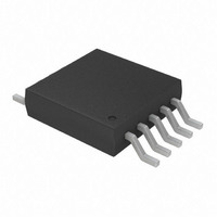
... Package Marking Information 8-Lead DFN (3x3) (MCP652) XXXX YYWW NNN 8-Lead SOIC (150 mil) (MCP651, MCP652) XXXXXXXX XXXXYYWW NNN 10-Lead DFN (3x3) (MCP655) XXXX YYWW NNN 10-Lead MSOP (MCP655) XXXXXX YWWNNN Legend: XX...X Customer-specific information Y Year code (last digit of calendar year) ...
Page 32
... MCP651/2/5 /HDG 3ODVWLF 'XDO )ODW 1R /HDG 3DFNDJH 0) ± 1RWH D N NOTE TOP VIEW A3 1RWHV DS22146A-page 32 PP %RG\ >')1@ b EXPOSED PAD E K BOTTOM VIEW A NOTE NOTE © 2009 Microchip Technology Inc. ...
Page 33
... Microchip Technology Inc. MCP651/2/5 PP %RG\ >')1@ DS22146A-page 33 ...
Page 34
... MCP651/2/5 /HDG 3ODVWLF 6PDOO 2XWOLQH 61 ± 1DUURZ 1RWH N NOTE 1RWHV DS22146A-page 34 PP %RG\ >62,& φ α c β © 2009 Microchip Technology Inc. ...
Page 35
... Microchip Technology Inc. MCP651/2/5 PP %RG\ >62,&@ DS22146A-page 35 ...
Page 36
... MCP651/2/5 /HDG 3ODVWLF 'XDO )ODW 1R /HDG 3DFNDJH 0) ± 1RWH D N NOTE TOP VIEW A3 1RWHV DS22146A-page 36 PP %RG\ >') EXPOSED PAD BOTTOM VIEW A A1 NOTE NOTE © 2009 Microchip Technology Inc. ...
Page 37
... Microchip Technology Inc. MCP651/2/5 PP %RG\ >')1@ DS22146A-page 37 ...
Page 38
... MCP651/2/5 /HDG 3ODVWLF 0LFUR 6PDOO 2XWOLQH 3DFNDJH 81 >0623@ 1RWH D N NOTE 1RWHV DS22146A-page φ © 2009 Microchip Technology Inc. ...
Page 39
... APPENDIX A: REVISION HISTORY Revision A (April 2009) • Original Release of this Document. © 2009 Microchip Technology Inc. MCP651/2/5 DS22146A-page 39 ...
Page 40
... MCP651/2/5 NOTES: DS22146A-page 40 © 2009 Microchip Technology Inc. ...
Page 41
... Extended Temperature, 8LD SOIC package. a) MCP652T-E/MF: Tape and Reel, Extended Temperature, 8LD DFN package. b) MCP652T-E/SN: Tape and Reel, Extended Temperature, 8LD SOIC package. a) MCP655T-E/MF: Tape and Reel, Extended Temperature, 10LD DFN package. b) MCP655T-E/UN: Tape and Reel, Extended Temperature, 10LD MSOP package. DS22146A-page 41 ...
Page 42
... MCP651/2/5 NOTES: DS22146A-page 42 © 2009 Microchip Technology Inc. ...
Page 43
... PowerMate, PowerTool, REAL ICE, rfLAB, Select Mode, Total Endurance, WiperLock and ZENA are trademarks of Microchip Technology Incorporated in the U.S.A. and other countries. SQTP is a service mark of Microchip Technology Incorporated in the U.S.A. All other trademarks mentioned herein are property of their respective companies. ...
Page 44
... Fax: 886-3-6578-370 Taiwan - Kaohsiung Tel: 886-7-536-4818 Fax: 886-7-536-4803 Taiwan - Taipei Tel: 886-2-2500-6610 Fax: 886-2-2508-0102 Thailand - Bangkok Tel: 66-2-694-1351 Fax: 66-2-694-1350 © 2009 Microchip Technology Inc. EUROPE Austria - Wels Tel: 43-7242-2244-39 Fax: 43-7242-2244-393 Denmark - Copenhagen Tel: 45-4450-2828 Fax: 45-4485-2829 France - Paris Tel: 33-1-69-53-63-20 ...