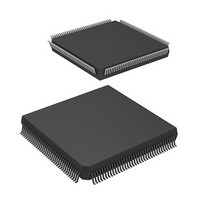
DF2338VFC25IV Renesas Electronics America, DF2338VFC25IV Datasheet - Page 707

DF2338VFC25IV
Manufacturer Part Number
DF2338VFC25IV
Description
MCU 3V 256K I-TEMP PB-FREE 144-Q
Manufacturer
Renesas Electronics America
Series
H8® H8S/2300r
Specifications of DF2338VFC25IV
Core Processor
H8S/2000
Core Size
16-Bit
Speed
25MHz
Connectivity
SCI, SmartCard
Peripherals
DMA, POR, PWM, WDT
Number Of I /o
106
Program Memory Size
256KB (256K x 8)
Program Memory Type
FLASH
Ram Size
8K x 8
Voltage - Supply (vcc/vdd)
2.7 V ~ 3.6 V
Data Converters
A/D 12x10b; D/A 4x8b
Oscillator Type
Internal
Operating Temperature
-40°C ~ 85°C
Package / Case
144-QFP
Lead Free Status / RoHS Status
Lead free / RoHS Compliant
Eeprom Size
-
- Current page: 707 of 1246
- Download datasheet (7Mb)
15.2.4
In smart card interface mode, the function of bits 1 and 0 of SCR changes when bit 7 of the serial
mode register (SMR) is set to 1.
Bits 7 to 2—Operate in the same way as for the normal SCI. For details, see section 14.2.6, Serial
Control Register (SCR).
Bits 1 and 0—Clock Enable 1 and 0 (CKE1, CKE0): These bits are used to select the SCI clock
source and enable or disable clock output from the SCK pin.
In smart card interface mode, in addition to the normal switching between clock output enabling
and disabling, the clock output can be specified as being fixed high or low.
SMIF
0
1
1
1
1
1
1
Bit
Initial value :
R/W
SCMR
Serial Control Register (SCR)
GM
See the SCI specification
0
0
1
1
1
1
:
:
SMR
R/W
TIE
7
0
CKE1
0
0
0
0
1
1
R/W
RIE
6
0
SCR Setting
R/W
CKE0
0
1
0
1
0
1
TE
5
0
R/W
RE
0
4
SCK Pin Function
Operates as port I/O pin
Outputs clock as SCK output pin
Operates as SCK output pin, with output fixed
low
Outputs clock as SCK output pin
Operates as SCK output pin, with output fixed
high
Outputs clock as SCK output pin
Rev.4.00 Sep. 07, 2007 Page 675 of 1210
MPIE
R/W
3
0
TEIE
R/W
2
0
REJ09B0245-0400
CKE1
R/W
1
0
CKE0
R/W
0
0
Related parts for DF2338VFC25IV
Image
Part Number
Description
Manufacturer
Datasheet
Request
R

Part Number:
Description:
KIT STARTER FOR M16C/29
Manufacturer:
Renesas Electronics America
Datasheet:

Part Number:
Description:
KIT STARTER FOR R8C/2D
Manufacturer:
Renesas Electronics America
Datasheet:

Part Number:
Description:
R0K33062P STARTER KIT
Manufacturer:
Renesas Electronics America
Datasheet:

Part Number:
Description:
KIT STARTER FOR R8C/23 E8A
Manufacturer:
Renesas Electronics America
Datasheet:

Part Number:
Description:
KIT STARTER FOR R8C/25
Manufacturer:
Renesas Electronics America
Datasheet:

Part Number:
Description:
KIT STARTER H8S2456 SHARPE DSPLY
Manufacturer:
Renesas Electronics America
Datasheet:

Part Number:
Description:
KIT STARTER FOR R8C38C
Manufacturer:
Renesas Electronics America
Datasheet:

Part Number:
Description:
KIT STARTER FOR R8C35C
Manufacturer:
Renesas Electronics America
Datasheet:

Part Number:
Description:
KIT STARTER FOR R8CL3AC+LCD APPS
Manufacturer:
Renesas Electronics America
Datasheet:

Part Number:
Description:
KIT STARTER FOR RX610
Manufacturer:
Renesas Electronics America
Datasheet:

Part Number:
Description:
KIT STARTER FOR R32C/118
Manufacturer:
Renesas Electronics America
Datasheet:

Part Number:
Description:
KIT DEV RSK-R8C/26-29
Manufacturer:
Renesas Electronics America
Datasheet:

Part Number:
Description:
KIT STARTER FOR SH7124
Manufacturer:
Renesas Electronics America
Datasheet:

Part Number:
Description:
KIT STARTER FOR H8SX/1622
Manufacturer:
Renesas Electronics America
Datasheet:

Part Number:
Description:
KIT DEV FOR SH7203
Manufacturer:
Renesas Electronics America
Datasheet:


